SiGe Differential Amplifier Drives High Speed ADCs at Hundreds of MHz
SiGe Differential Amplifier Drives High Speed ADCs at Hundreds of MHz
2007年06月01日
Introduction
The last few years have seen great advances in the performance of analog-to-digital converters. Sampling rates for 12-, 14- and even 16-bit ADCs are now well above 100Msps. The LTC6400 differential amplifier has been specifically designed to drive these high performance ADC inputs in a way that maintains their excellent low noise and high linearity performance, all while operating off a low 3V or 3.3V supply voltage.
IF Sampling
In addition to the higher sample rates, the analog input frequency range of ADCs has been greatly expanded as well. Long gone are the days when you could only use an ADC with input frequencies no greater than half the sample rate. Is Harry Nyquist turning over in his grave, you ask? Not exactly. It is still generally a good idea to limit the total signal bandwidth that gets digitized to one-half of the sample rate. However, nobody says that you have to place that swath of bandwidth starting at DC. For example, with a 100Msps ADC, you can digitize signals that are bandpass limited between 150MHz and 200MHz. The total bandwidth is still 50MHz, which is half the sample rate, but the input frequencies at which you operate are much higher.
In modern communications receiver systems, the practice described above is called IF sampling or undersampling. The RF input signal is mixed down to an IF frequency using a downconverting mixer such as the LT5557. This IF frequency is digitized, and all further processing is done digitally. To make this work for the high performance receiver systems in tomorrow’s wireless basestations, the analog signal path that processes the IF frequency must be highly linear and low noise. The LTC6400 fills that need in a way that is efficient both in terms of board space and power.
Performance without Precedent
Figure 1 shows the intermodulation distortion vs input frequency for a 2VP–P output signal. The LTC6400 achieves distortion at the –90dBc level up to 140MHz, and at the –70dBc level up to a couple hundred MHz. Previously, this type of performance was only achievable using much higher power RF gain blocks (which typically aren’t even differential). Figure 2 shows the equivalent OIP3 (3rd order output intercept point), which is an RF figure-of-merit that expresses output linearity irrespective of signal level.


Figure 1. The LTC6400 maintains low intermodulation distortion up to hundreds of MHz, allowing for high performance IF sampling applications.

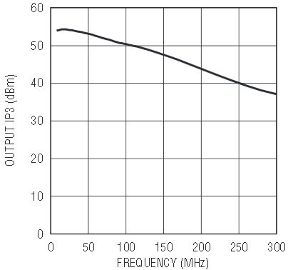
Figure 2. The LTC6400 Equivalent Output-IP3 is in excess of 50dBm up to 100MHz, and in excess of 40dBm up to 250MHz.
Besides distortion, the other key performance requirement of an IF ADC Driver is low noise contribution. The LTC6400 is based on a differential op amp with a very quiet 1nV/√Hz input noise density. The internal 200Ω differential input resistors inevitably add some noise of their own, resulting in a 2.1nV/√Hz total input referred noise density.
In RF terms, when terminated in a matched 200Ω system, this translates to a noise figure of only 6.1dB. Since the LTC6400 is typically the last stage before the ADC in a receiver line-up there are other gain blocks that precede it. To refer a component’s noise contribution to the actual input of the entire receiver, you divide it by the gain that precedes it. Therefore, the low 6.1dB noise figure of the LTC6400 allows for very low noise receiver designs.
Another way to look at noise is in terms of SNR (signal-to-noise ratio). The LTC6400-20 output noise density is 21nV/√Hz (because the gain is 10V/V). If you limit the input signal bandwidth to a generous 50MHz, this amounts to 148μVRMS of integrated noise. This allows for a 74dB SNR relative to a 2VP-P full-scale signal, compatible with popular 14-bit ADCs such as the LTC2249.
A Look under the Hood
The LTC6400 differential amplifier is manufactured on an advanced complementary bipolar silicon-germanium (SiGe) process. Because germanium atoms are larger than silicon atoms, selectively adding some germanium to an otherwise silicon process causes strains within the material’s crystalline structure. This strain actually results in beneficial electrical properties, such as higher carrier mobility and a more precise control of the base-width, allowing for faster transistors.
Figure 3 shows a block diagram of the LTC6400. At its core is a very high speed differential op amp. The combination of fast transistors and streamlined circuit topology results in an op amp with a gain-bandwidth product in excess of 3GHz relative to a unity-gain stable transfer function. Furthermore, all feedback resistors are integrated. In addition to the obvious space savings, integrating the feedback network results in several design benefits:
- The sensitive summing nodes at the immediate inputs of the op amp are not exposed to the vagaries of board layout, which allows us to carefully control the amount of parasitic capacitance seen at that node. Otherwise, even as little as 100 femto-Farads at this node (for example due to board traces, package pins, or bond pads) would cause unwanted poles in the loop-gain of the feedback network.
- If the feedback resistors were off-chip, two sets of bond wires (at the op amp outputs and inputs) would be in the feedback loop. On chip resistors eliminate bond wire or lead inductance associated with the op amp inputs, and those at the op amp outputs are outside of the feedback loop. At frequencies of 3GHz and above, even a small 1nH of inductance exhibits significant impedance and phase shift, which would again limit the achievable speed and performance.
- Since the gain is fixed and higher than unity, we can internally de-compensate the op amp to achieve the maximum possible open-loop gain for a given closed-loop configuration. The more open-loop gain, the better the feedback action can suppress non-linear components. In addition, this compensation technique preserves a wide –3dB bandwidth even though the gain is high, as shown in Figure 4.


Figure 3. The LTC6400 combines a very high speed differential op amp with on-chip feedback resistors.


Figure 4: The op amp inside the LTC6400-20 is internally decompensated, so that even though the closed loop gain is 10V/V (20dB), the closed loop –3dB bandwidth is still an impressive 1.8GHz.
Application Example
Figure 5 shows a typical application of the LTC6400 driving the LTC2208, a 16-Bit 130Msps ADC. In this case, the input signal is single-ended, and applied to the +IN input of the LTC6400 through a DC-blocking capacitor. (With a little bit of care, the signal could also be DC-coupled, so long as the DC voltage is within the input common mode range of the amplifier.) As can be readily observed from Figure 3, the input impedance of the LTC6400-20 is 200Ω differential. The 66.5Ω input resistor changes the total input impedance to 50Ω, to provide a match to a 50Ω source impedance. Alternatively, a 1:4 transformer may be used for matching the amplifier to a 50Ω load. In other cases, the source impedance may already be 200Ω and no additional components would be necessary. The 29Ω resistor placed at the –IN input provides a balanced termination for the internal op amp.


Figure 5. The LTC6400 can drive high performance ADCs with a minimum of external components.
The LTC6400 is powered from the same 3.3V as the ADC, saving the need for another power supply rail. It could do the same with a 3V rail. Other driver solutions require 5V or more to drive ADCs to full-scale with high performance.
The LTC2208 family of ADCs wants to see its inputs swing centered around a 1.25V common mode voltage. The LTC6400 makes this easy: simply connect the VCM pin of the ADC to the VOCM pin of the LTC6400, and the amplifier’s internal common-mode feedback loop ensures that the outputs swing centered around the value applied to VOCM. For ADCs that prefer a 1.5V common-mode voltage, the interface is the same.
Related Parts
The LTC6401-20 is a lower power version of the LTC6400-20. The LTC6401-20 consumes only 45mA at 3V or 3.3V. Both amplifiers are pin-compatible and have the same low noise performance. The LTC6401 maintains excellent linearity up to 140MHz, while consuming only half the power of the LTC6400.
Conclusion
By combining a new SiGe process with careful, innovative design, the LTC6400 offers unprecedented performance at high frequencies, all while operating at a low 3V or 3.3V supply voltage. A tiny 9mm2 leadless package, along with a minimal number of external components, lets you place the driver right at the ADC inputs, providing the best performance and compact board layout. The differential outputs are uniquely optimized to directly drive state-of-the art high speed ADCs with high linearity, while the low input-noise preserves the sensitivity of a high performance receiver system.
著者について
Kris Lokereは、シグナル・チェーン製品の戦略的アプリケーション・マネージャで、リニア・テクノロジーの買収に伴いアナログ・デバイセズに入社しました。複数の製品ラインの技術を組み合わせるシステムを設計することに取り組んでいます。過去20年間に、オペアンプの設計、エンジニアリング・チームの構築、製品ライン戦略の管理に従事してきました。複数の特許を保有し、また、ルーヴェン・カトリック大学でM.S.E.E、バブソン大学でM.B.Aの学位を取...
この記事に関して
最新メディア 21