要約
Low-dropout LDO linear regulators are used to power many sections of a typical cellular handset. However, these baseband, RF, and audio sections have different requirements that influence which LDO is most appropriate. After discussion of the specific requirements, different LDOs are recommended. Also, some LDO design techniques are briefly discussed to demonstrate how an LDO may be optimized for a specific level of performance.
Cellular phone designs require linear regulators with low-dropout, low-noise, high PSRR, low quiescent current (Iq), and low-cost. They need to deliver a stable output and use small-value output capacitors.
Ideally, one device would have all these characteristics and one low-dropout linear regulator (LDO) could be used anywhere in the phone without worry. But in practice, the various cell phone blocks are best powered by LDOs with different performance characteristics. This application note provides guidance in choosing the right LDO to power each cell phone block.
Baseband Chipset Power Supply
Most cellular phone baseband chipsets require power supplies for three circuit blocks: internal digital circuitry, analog circuitry, and peripheral interface circuitry. BB internal digital circuits typically operate from 1.8V to 2.6V. Since most phones shut off when the Li+ battery voltage falls to 3.2V to 3.3V, there is usually at least 500mV to 600mV of headroom for the BB digital LDO, so dropout is not critical. Output noise and the PSRR are not critical specs for the digital circuits. Instead, this supply requires low quiescent current at light loads because this LDO stays on at all times. Figure 1 shows how the digital supply current of a representative GSM chipset core (ADI AD20msp425) varies as a function of time. In the standby mode, the microprocessor consumes only around 200µA. Since the phone stays in standby for the longest percentage of time, using a 2µA quiescent current LDO, instead of 100µA LDO, saves 98µA and extends the standby time by 300µA /202µA, or 1.485 times.
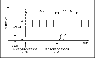
Figure 1. ADI AD20msp425 GSM chipset core power consumption profile.
The supply voltage of the BB internal analog circuits is typically 2.4V to 3.0V, and it requires 200mV to 600mV dropout. Also, the BB analog LDO needs to be optimized for low-frequency (217Hz for GSM phones) ripple rejection in order to reject the battery voltage ripple caused by the RF power amplifier. This LDO is on all the time, so it requires low quiescent current as well.
RF Power Supply
The RF circuit is divided into receive and transmit sections. These circuits typically require 2.6V to 3.0V supply voltage. The RF circuits such as LNA (low-noise amplifier), up/downconverter, mixer, PLL, VCO, and IF stage require low-noise and high PSRR LDOs. In particular, the VCO and PLL blocks' overall performance affects the radio's critical specifications, such as spectral purity of the transmitter, selectivity of the receiver, noise and hum in analog transceivers, and phase errors in digital circuits. Noise can alter the oscillator's phase and amplitude characteristic and the oscillator's loop circuitry amplifies the noise. Consequently, it may modulate the carrier. The LDO output noise can be reduced by effective LDO internal design and external bypass and compensation. Figure 2 shows a simplified block diagram of the PMOS linear regulator.
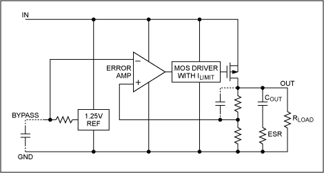
Figure 2. A simplified PMOS linear regulator block diagram.
The major contributor to LDO output noise is the reference. Figure 3 shows a typical bandgap reference noise spectrum.
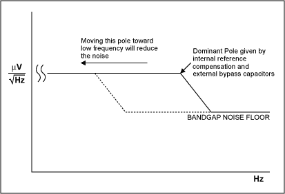
Figure 3. Typical noise spectrum of a bandgap reference.
In order to reduce the reference noise, a low pass filter needs to be added on the reference output. This can be done internally or externally, but the internal bypass may take a large die size. LDOs designed for low-noise will often provide a pin for a reference bypass capacitor. Increasing the bypass capacitor value will reduce the output noise up to a point where the reference noise becomes a minor noise contributor in overall LDO circuits. Output noise vs. bypass capacitance characteristics in the LDO data sheet will provide information for an optimum bypass capacitor value. Figure 4 shows output noise vs. BP capacitance of the MAX8867.
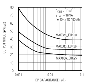
Figure 4. Output noise vs. BP capacitance of the MAX8867.
Other factors affecting the LDO output noise are LDO internal poles, zeros, and the output dominant pole. Figure 5 shows the typical noise spectrum of the PMOS linear regulator except the bandgap reference. By increasing the output capacitor's value or reducing output load, the high-frequency output noise will be reduced.When choosing an LDO for an RF circuit, carefully compare the noise specifications to make sure that the bypass capacitance, output capacitance, and load conditions are the same.
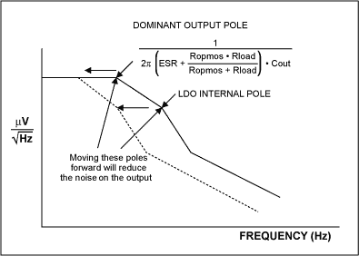
Figure 5. Typical noise spectrum of PMOS LDO except the bandgap reference.
TCXO Power Supply
The temperature-compensated crystal oscillator generates a reference frequency which is used for IF sections. It requires an ultra-low noise LDO with an on/off control pin. Even though the TCXO circuit does not require more than 5mA, it uses a dedicated LDO and isolates the LDO's output from other noise sources. It also requires very high PSRR at RF power amplifier burst frequency. For example, minimum 65dB PSRR at 217Hz is recommended for the GSM handsets.
RTC Power Supply
The RTC LDO charges a capacitor-type backup coin cell or a rechargeable coin cell and supplies current for a real-time clock (See Figure 6). 3V or 2.5V cells are the most common for cellular phones. The RTC LDO needs a very low quiescent current, since this LDO is on all the time, even though the handset is powered off. It also requires a reverse current protection with a low leakage current.
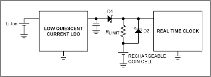
Figure 6. RTC and rechargeable coin cell.
Audio Power Supply
The 300mA to 500mA high current LDO may be required for recent audio demands such as hands-free, game, MP3, and multimedia applications in cellular phones. Also, this power supply requires low-noise and high PSRR at audio frequency range (20Hz to 20kHz) in order to provide good audio quality. CDMA RF transmit current is around 600mA peak, but GSM transmit burst current is 1.7A peak. Figure 7 shows how the GSM transmit burst current creates noise on the battery when the RF power amplifier runs directly from the battery. Since all LDOs in the phones use the battery voltage for their input power source, this ripple influences output quality of the regulators. For example, if the LDO's PSRR at 217Hz is 40dB, we will have 4.35mV peak-to-peak, 217Hz noise on the LDO output based on Figure 7. The microphone's AC audio level is around 10mV to 20mV, so this noise may cause a serious clicking noise.
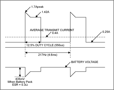
Figure 7. GSM transmit burst waveform.
Maxim LDOs for Cellular Phone Applications
The following table summarizes the Maxim LDO product line suitable for the wireless phone applications.
| Part numbers | Package | Dropout | Ground current | Output noise | PSRR | Application area | Remark |
| MAX8863 MAX8864 |
SOT23-5 | 55mV at 50mA | 68µA | 350µVRMS at 10Hz–1MHz, COUT = 1µF | 62dB at 300Hz | BB Digital | |
| MAX8867 MAX8868 |
SOT23-5 | 55mV at 50mA | 85µA | >30µVRMS at 10Hz–100kHz, COUT = 10µF, CBYP = 0.01µF | > 60dB at 10Hz–100kHz | Audio BB Analog BB Digital RF Circuit |
|
| MAX8873 MAX8874 (Auto Discharge) |
SOT23-5 | 55mV at 50mA | 73µA at no load |
350µVRMS at 10Hz–1MHz, COUT = 1µF | 60dB at 300Hz | BB Digital | |
| MAX8877 MAX8878 (Auto Discharge) |
SOT23-5 | 55mV at 50mA | 85µA at no load |
30µVRMS at 10Hz–100kHz, COUT = 10µF, CBYP = 0.01µF | 60dB at 300Hz | Audio BB Analog BB Digital RF Circuit |
|
| MAX8875 MAX8885 (Auto Discharge) |
SOT23-5 | 55mV at 50mA | 85µA at no load |
30µVRMS at 10Hz–100kHz, COUT = 10µF, CBYP = 0.01µF | 60dB at 300Hz | Audio BB Analog BB Digital RF Circuit |
|
| MAX8887 | Thin SOT23-5 | 100mV at 200mA | 55µA at no load |
42µVRMS at 10Hz–100kHz, COUT = 2.2µF, CBYP = 0.01µF | 60dB below 1kHz with COUT = 2.2µF, CBYP = 0.01µ | Audio BB Analog BB Digital RF Circuit |
300mA |
| MAX8882 | SOT23-6 | 72mV at 80mA | 165µA at no load |
40µVRMS at 10Hz–100kHz, COUT = 4.7µF, CBYP = 0.01µF, IOUT = 1mA | 62dB at 300Hz 56dB up to 100kHz | BB Analog BB Digital RF Circuit |
Dual LDO |
| MAX1725 MAX1726 |
SOT23-5 | 300mV at 20mA | 2µA at no load |
350µVRMS at 10Hz–100kHz, COUT = 4.7µF, IOUT = 1µA | 45dB at 300Hz | RTC Circuit | |
| MAX8880 MAX8881 |
SOT23-5 | 100mV at 50mA | 3.5µA at no load |
300µVRMS at 10Hz–100kHz, COUT = 4.7µF, IOUT = 1µA | 45dB at 300Hz | BB Digital RTC circuit |
この記事に関して
最新メディア 21