クイックスタート:MAX6954を使って7セグメントディスプレイを駆動
要約
このアーティクルは、MAX6954を使用して7セグメントのモノカラーLEDを駆動することを検討している技術者が迅速に学ぶことを目的に作られたガイドブックです。
MAX6954は汎用のディスプレイドライバであり、シリアルインタフェースを通して、個別の7セグメント、14セグメント、および16セグメントLEDディスプレイを混在して駆動することができます。このアプリケーションノートでは、MAX6954を用いて16個のモノカラー、7セグメンントのLEDを駆動するための標準的なアプリケーションと構成を示します。
MAX6954の機能の詳細についてはMAX6954のデータシートをご覧ください。
「クイックスタート:MAX6954を使って16セグメントディスプレイを駆動する」および「クイックスタート:MAX6954を使って14セグメントディスプレイを駆動」は、MAX6954を16セグメントおよび14セグメントのアプリケーションを構成することを述べた同様のアプリケーションノートです。
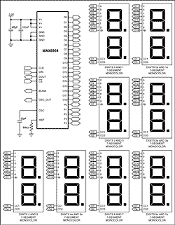
図1. MAX6954の7セグメントアプリケーション回路
MAX6954の標準的なアプリケーションの一例は、最大16個の7セグメントモノカラーLEDの駆動です。このアプリケーションノートでは、MAX6954を7セグメントディスプレイに接続し、内蔵の16進フォントマップを使ってディスプレイを制御するための内部レジスタを構成するプロセスを、ユーザに解説します。
MAX6954はマルチプレクス技術を使用します。これは使用するポートのピン数を少なくして、これを交互にカソードとアノードドライバとして使うものです。これはアノード用とカソード用に別のドライバを用いる標準的なLEDマルチプレクス接続とは異なります。この技術は「Charlieplexing - Reduced Pin-Count LED Display Multiplexing」にて説明されています。表1はMAX6954マルチプレクス方式に対応した7セグメントの各桁の接続方法と内蔵の16進のフォントマップを示しています。表1における文字は図2に示したセグメントラベルに対応しています。図1はMAX6954に対する16桁の7セグメントのアプリケーションを図示しています。
| Digit | O0 | O1 | O2 | O3 | O4 | O5 | O6 | O7 | O8 | O9 | O10 | O11 | O12 | O13 | O14 | O15 | O16 | O17 | O18 |
| 0 0a |
CC0 | 1a | 1b | 1c | 1d | 1dp | 1e | 1f | 1g | 2a | 2b | 2c | 2d | 2e | 2f | 2g | 2dp | ||
| 1, 1a |
CC1 | 1a | 1b | 1c | 1d | 1dp | 1e | 1f | 1g | 2a | 2b | 2c | 2d | 2e | 2f | 2g | 2dp | ||
| 2, 2a |
1a | CC2 | 1b | 1c | 1d | 1dp | 1e | 1f | 1g | 2a | 2b | 2c | 2d | 2e | 2f | 2g | 2dp | ||
| 3 3a |
1a | CC3 | 1b | 1c | 1d | 1dp | 1e | 1f | 1g | 2a | 2b | 2c | 2d | 2e | 2f | 2g | 2dp | ||
| 4 4a |
1a | 1b | 1c | CC4 | 1d | 1dp | 1e | 1f | 1g | 2a | 2b | 2c | 2d | 2e | 2f | 2g | 2dp | ||
| 5 5a |
1a | 1b | 1c | CC5 | 1d | 1dp | 1e | 1f | 1g | 2a | 2b | 2c | 2d | 2e | 2f | 2g | 2dp | ||
| 6, 6a |
1a | 1b | 1c | 1d | 1dp | CC6 | 1e | 1f | 1g | 2a | 2b | 2c | 2d | 2e | 2f | 2g | 2dp | ||
| 7, 7a |
1a | 1b | 1c | 1d | 1dp | CC7 | 1e | 1f | 1g | 2a | 2b | 2c | 2d | 2e | 2f | 2g | 2dp |
MAX6954を7セグメントのディスプレイに接続した後、接続を確認するためにディスプレイのテストモードを使うことができます。ディスプレイのテストモードはすべての制御用レジスタと桁レジスタに優先して、しかしその内容を変更することなく、すべてのセグメントをオンとします。0x01をレジスタ0x07に書き込むことによってディスプレイテストモードをイネーブルとしてください。ディスプレイテストモードでセグメントが点灯しない場合は、接続に問題があるため調べる必要があります。0x00をレジスタ0x07に書き込むとディスプレイテストモードを解除します。
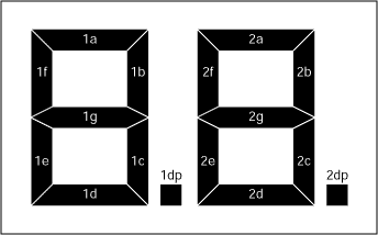
図2. 7セグメントディスプレイのためのセグメントラベリング
MAX6954と7セグメントディスプレイ間の接続確認が終わった後、デバイスは7セグメントディスプレイとして動作するように構成しなければなりません。表2はMAX6954の重要なレジスタの電源投入時の初期状態リストです。電源がMAX6954に最初に印加されたとき、デバイスはシャットダウンモードとなっており、すべての桁は消灯(ブランク)であり、7セグメントのフォントマップが選択されてデバイスは最大桁をスキャンするようにセットされています。Decode Mode (0x01)およびDigit Type (0x0C)レジスタのデフォルト設定値は7セグメントにとって、正しい設定となっています。
| REGISTER | POWER-UP CONDITION | ADDRESS (HEX) |
REGISTER DATA | |||||||
| D7 | D6 | D5 | D4 | D3 | D2 | D1 | D0 | |||
| Decode Mode | 7-segment font enabled | 0x01 | 1 | 1 | 1 | 1 | 1 | 1 | 1 | 1 |
| Global Intensity | 1/16 (minimum intensity) | 0x02 | X | X | X | X | 0 | 0 | 0 | 0 |
| Scan Limit | Display sixteen 7-segment digits: 0, 1, 2, 3, 4, 5, 6, 7, 0a, 1a, 2a, 3a, 4a, 5a, 6a, 7a | 0x03 | X | X | X | X | X | 1 | 1 | 1 |
| Control Register | Shutdown enabled, blink disabled, blink speed is slow | 0x04 | 0 | 0 | X | X | 0 | 0 | 0 | 0 |
| Display Test | Normal operation (display test disabled) | 0x07 | X | X | X | X | X | X | X | 0 |
| Digit Type | Digits 0 through 7 are 7 segment digits | 0x0C | 0 | 0 | 0 | 0 | 0 | 0 | 0 | 0 |
| Intensity10 | 1/16 (min on), digits 1 and 0 | 0x10 | 0 | 0 | 0 | 0 | 0 | 0 | 0 | 0 |
| Intensity32 | 1/16 (min on), digits 3 and 2 | 0x11 | 0 | 0 | 0 | 0 | 0 | 0 | 0 | 0 |
| Intensity54 | 1/16 (min on), digits 5 and 4 | 0x12 | 0 | 0 | 0 | 0 | 0 | 0 | 0 | 0 |
| Intensity76 | 1/16 (min on), digits 7 and 6 | 0x13 | 0 | 0 | 0 | 0 | 0 | 0 | 0 | 0 |
| Intensity10a | 1/16 (min on), digits 1a and 0a | 0x14 | 0 | 0 | 0 | 0 | 0 | 0 | 0 | 0 |
| Intensity32a | 1/16 (min on), digits 3a and 2a | 0x15 | 0 | 0 | 0 | 0 | 0 | 0 | 0 | 0 |
| Intensity54a | 1/16 (min on), digits 5a and 4a | 0x16 | 0 | 0 | 0 | 0 | 0 | 0 | 0 | 0 |
| Intensity76a | 1/16 (min on), digits 7a and 6a | 0x17 | 0 | 0 | 0 | 0 | 0 | 0 | 0 | 0 |
| Digit 0 | Blank digit, both planes | 0x60 | 0 | 0 | 1 | 0 | 0 | 0 | 0 | 0 |
| Digit 1 | Blank digit, both planes | 0x61 | 0 | 0 | 1 | 0 | 0 | 0 | 0 | 0 |
| Digit 2 | Blank digit, both planes | 0x62 | 0 | 0 | 1 | 0 | 0 | 0 | 0 | 0 |
| Digit 3 | Blank digit, both planes | 0x63 | 0 | 0 | 1 | 0 | 0 | 0 | 0 | 0 |
| Digit 4 | Blank digit, both planes | 0x64 | 0 | 0 | 1 | 0 | 0 | 0 | 0 | 0 |
| Digit 5 | Blank digit, both planes | 0x65 | 0 | 0 | 1 | 0 | 0 | 0 | 0 | 0 |
| Digit 6 | Blank digit, both planes | 0x66 | 0 | 0 | 1 | 0 | 0 | 0 | 0 | 0 |
| Digit 7 | Blank digit, both planes | 0x67 | 0 | 0 | 1 | 0 | 0 | 0 | 0 | 0 |
| Digit 0a | Blank digit, both planes | 0x68 | 0 | 0 | 1 | 0 | 0 | 0 | 0 | 0 |
| Digit 1a | Blank digit, both planes | 0x69 | 0 | 0 | 1 | 0 | 0 | 0 | 0 | 0 |
| Digit 2a | Blank digit, both planes | 0x6A | 0 | 0 | 1 | 0 | 0 | 0 | 0 | 0 |
| Digit 3a | Blank digit, both planes | 0x6B | 0 | 0 | 1 | 0 | 0 | 0 | 0 | 0 |
| Digit 4a | Blank digit, both planes | 0x6C | 0 | 0 | 1 | 0 | 0 | 0 | 0 | 0 |
| Digit 5a | Blank digit, both planes | 0x6D | 0 | 0 | 1 | 0 | 0 | 0 | 0 | 0 |
| Digit 6a | Blank digit, both planes | 0x6E | 0 | 0 | 1 | 0 | 0 | 0 | 0 | 0 |
| Digit 7a | Blank digit, both planes | 0x6F | 0 | 0 | 1 | 0 | 0 | 0 | 0 | 0 |
- Sビットはシャットダウンまたは通常動作を選択します(リード/ライト可能)。
- Bビットはブリンク速度を選択します(リード/ライト可能)。
- Eビットは全桁のブリンク機能を許可/禁止としてイネーブルまたは(リード/ライト可能)。
- Tビットはブリンクタイミングをリセット(過渡ビットであり、記憶されません)。
- Rビットによってすべての桁のP0とP1の両面の桁データをクリア(過渡ビットであり、記憶されません)。
- Iビットは全体または桁ごとの輝度を選択(リード/ライト可能)。
- Pビットは現在のブリンクタイミング位相を反映(リード専用、このビットへのライトは無視されます)。
| CONFIGURATION REGISTER DATA BIT |
DATA BIT LABEL | STATE | FUNCTION |
| D7 | P | 0 | P1 Blink Phase |
| D6 | I | 0 | Intensity for all digits is controlled by one setting in the Global Intensity Register |
| 1 | Intensity for digits is controlled by the individual settings in the Intensity10 through Intensity76a registers. | ||
| D5 | R | 0 | Digit data for both planes P0 and P1 are unaffected |
| 1 | Digit data for both planes P0 and P1 are cleared on the rising edge of active-low CS | ||
| D4 | T | 0 | Blink timing counters are unaffected. |
| 1 | Blink timing counters are reset on the rising edge of active-low CS. | ||
| D3 | E | 0 | Blink function disabled |
| 1 | Blink function enabled | ||
| D2 | B | 0 | Slow Blinking. Segments blink on for 1s, off for 1s with fOSC = 4MHz. |
| 1 | Fast Blinking. Segments blink on for 0.5s, off for 0.5s with fOSC = 4MHz. | ||
| D1 | X | X | Don't care |
| D0 | S | 0 | Shutdown |
| 1 | Normal Operation |
レジスタ0x04に0x01を書き込むことによってブリンクさせるのではなく、全体の輝度制御をディスプレイドライバに許可してください。MAX6954がシャットダウンから抜け出して内蔵の発振器が給電されると、OSC_OUT発振器出力が有効になります。このとき、まだ、7セグメントディスプレイは消灯のままです。それは桁制御レジスタ0x60~0x6Fの電源投入時の状態は0x20、または点灯セグメントなしの状態だからです(表2と図3を参照してください)。
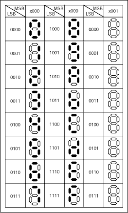
図3. 7セグメントディスプレイのフォントマップ"
MAX6954は7セグメントディスプレイ用の16進フォントマップを持っています。文字は標準のASCIIフォントに従います。7ビットが16進フォントマップを表現するために使われ、8番目のビットは少数点(DP)を点灯させるかどうかを選択します(表4)。桁レジスタは2つの面、P0とP1が実装されています。各桁は2バイトのメモリで表現され、1バイトがP0面にそしてもう1バイトがP1面にあります(表7を参照)。桁レジスタは桁データがP0面(レジスタ0x20~0x2F)、P1面(レジスタ0x40~0x4F)、または両面(レジスタ0x60~0x6F)同時に更新することができるようにマッピングされています。桁レジスタの中のデータは、7セグメントディスプレイの場合は桁セグメントを直接制御せず、7セグメントのフォント用のデータを格納する文字ジェネレータ器のアドレス指定のために使用されます(図3)。桁データの下位7ビット(D6~D0)は、フォントから文字データを選択します。このレジスタデータの最上位ビット(D7)は桁のDPセグメントを制御します;1の設定でDP点灯、0で消灯します。
| MODE | ADDRESS CODE (HEX) | REGISTER DATA | ||||||||
| D7 | D6 | D5 | D4 | D3 | D2 | D1 | D0 | |||
| 7-segment mode, writing digit data to use font map data with decimal place unlit | 0x20 to 0x2F 0x40 to 0x4F 0x60 to 0x6F |
0 | Bits D6 to D0 select font character | |||||||
| 7-segment mode, writing digit data to use font map data with decimal place lit | 0x20 to 0x2F 0x40 to 0x4F 0x60 to 0x6F |
1 | Bits D6 to D0 select font character | |||||||
コンフィギュレーションレジスタのブリンクイネーブルビットE (表3)によってブリンク機能がディセーブルされている場合、P0面の桁レジスタデータはディスプレイをマルチプレクスするために使われます。P1にある桁レジスタデータは使われません。ブリンク機能がイネーブルとされている場合、P0面とP1面の両方の桁レジスタデータはディスプレイをマルチプレクスするために交互に使われます。ブリンキングはデータP0面とP1面のデータを用いてLEDディスプレイをマルチプレクスすることによって行われます。
例として、MAX6954を用いて、Maxim/Dallas Directの電話番号:1 800 629 4642 begin_of_the_skype_highlighting 1 800 629 4642 end_of_the_skype_highlightingを表示して見ましょう。コンフィギュレーションレジスタをプログラムしたとき、ブリンク機能をディセーブルとしたので、データは桁0から桁7aを制御するために0x20~0x2Fレジスタに書き込むことができます。図3のフォントマップを用いて各文字と等価なコードを決定します。
| REGISTER ADDRESS (HEX) | DIGIT | CHARACTER | FONT MAP EQUIVALENT CODE | |
| DECIMAL | HEX | |||
| 0x20 | 0 | C | 0000 1100 | 0x0C |
| 0x28 | 0a | A | 0000 1001 | 0x0A |
| 0x21 | 1 | 1 | 0000 0001 | 0x01 |
| 0x29 | 1a | 1 | 0000 0001 | 0x01 |
| 0x23 | 3 | 8 | 0000 1000 | 0x08 |
| 0x2B | 3a | 0 | 0000 0000 | 0x00 |
| 0x24 | 4 | 0 | 1000 0000 | 0x80 |
| 0x2C | 4a | 6 | 0000 0110 | 0x06 |
| 0x25 | 5 | 2 | 0000 0010 | 0x02 |
| 0x2D | 5a | 9 | 1000 1001 | 0x89 |
| 0x26 | 6 | 4 | 0000 0100 | 0x04 |
| 0x2E | 6a | 6 | 0000 0110 | 0x06 |
| 0x27 | 7 | 4 | 0000 0100 | 0x04 |
| 0x2F | 7a | 2 | 0000 0010 | 0x02 |
全体の輝度制御レジスタであるレジスタ0x02に書き込むことによってディスプレイの輝度を調整してください。輝度は0x00 (最小オン、1/16の電流)と0xFF (最大オン、15/16の電流)の間で調整することができます。ディスプレイの明るさのディジタル制御は、また、各桁を個別に管理することができます。桁の明るさの調整およびその他のGPIOやKey-Scanのような高度な機能についてはMAX6954のデータシートを参照してください。
| REGISTER (HEX) |
COMMAND (HEX) |
FUNCTION |
| 0x07 | 0x01 | Enter display test mode |
| 0x07 | 0x00 | Exit display test mode |
| 0x04 | 0x01 | Exit shutdown mode, disable blinking and select global intensity control |
| 0x20 | 0x0C | Write "C" to digit 0 |
| 0x28 | 0x0A | Write "A" to digit 0a |
| 0x21 | 0x01 | Write "1" to digit 1 |
| 0x29 | 0x01 | Write "1" to digit 1a |
| 0x23 | 0x08 | Write "8" to digit 3 |
| 0x2B | 0x00 | Write "0" to digit 3a |
| 0x24 | 0x80 | Write "0." to digit 4 |
| 0x2C | 0x06 | Write "6" to digit 4a |
| 0x25 | 0x02 | Write "2" to digit 5 |
| 0x2D | 0x89 | Write "9." to digit 5a |
| 0x26 | 0x04 | Write "4" to digit 6 |
| 0x2E | 0x06 | Write "6" to digit 6a |
| 0x27 | 0x04 | Write "4" to digit 7 |
| 0x2F | 0x02 | Write "2" to digit 7a |
| 0x02 | 0xFF | Set global intensity to full-scale |
| REGISTER | ADDRESS (COMMAND BYTE) | ADDRESS (HEX CODE) |
|||||||
| D15 | D14 | D13 | D12 | D11 | D10 | D9 | D8 | ||
| Decode Mode | R/active-low W | 0 | 0 | 0 | 0 | 0 | 0 | 1 | 0x01 |
| Global Intensity | R/active-low W | 0 | 0 | 0 | 0 | 0 | 1 | 0 | 0x02 |
| Scan Limit | R/active-low W | 0 | 0 | 0 | 0 | 0 | 1 | 1 | 0x03 |
| Configuration | R/active-low W | 0 | 0 | 0 | 0 | 1 | 0 | 0 | 0x04 |
| Display Test | R/active-low W | 0 | 0 | 0 | 0 | 1 | 1 | 1 | 0x07 |
| Digit Type | R/active-low W | 0 | 0 | 0 | 1 | 1 | 0 | 0 | 0x0C |
| Intensity 10 | R/active-low W | 0 | 0 | 1 | 0 | 0 | 0 | 0 | 0x10 |
| Intensity 32 | R/active-low W | 0 | 0 | 1 | 0 | 0 | 0 | 1 | 0x11 |
| Intensity 54 | R/active-low W | 0 | 0 | 1 | 0 | 0 | 1 | 0 | 0x12 |
| Intensity 76 | R/active-low W | 0 | 0 | 1 | 0 | 0 | 1 | 1 | 0x13 |
| Intensity 10a | R/active-low W | 0 | 0 | 1 | 0 | 1 | 0 | 0 | 0x14 |
| Intensity 32a | R/active-low W | 0 | 0 | 1 | 0 | 1 | 0 | 1 | 0x15 |
| Intensity 54a | R/active-low W | 0 | 0 | 1 | 0 | 1 | 1 | 0 | 0x16 |
| Intensity 76a | R/active-low W | 0 | 0 | 1 | 0 | 1 | 1 | 1 | 0x17 |
| Digit 0 Plane P0 | R/active-low W | 0 | 1 | 0 | 0 | 0 | 0 | 0 | 0x20 |
| Digit 1 Plane P0 | R/active-low W | 0 | 1 | 0 | 0 | 0 | 0 | 1 | 0x21 |
| Digit 2 Plane P0 | R/active-low W | 0 | 1 | 0 | 0 | 0 | 1 | 0 | 0x22 |
| Digit 3 Plane P0 | R/active-low W | 0 | 1 | 0 | 0 | 0 | 1 | 1 | 0x23 |
| Digit 4 Plane P0 | R/active-low W | 0 | 1 | 0 | 0 | 1 | 0 | 0 | 0x24 |
| Digit 5 Plane P0 | R/active-low W | 0 | 1 | 0 | 0 | 1 | 0 | 1 | 0x25 |
| Digit 6 Plane P0 | R/active-low W | 0 | 1 | 0 | 0 | 1 | 1 | 0 | 0x26 |
| Digit 7 Plane P0 | R/active-low W | 0 | 1 | 0 | 0 | 1 | 1 | 1 | 0x27 |
| Digit 0a Plane P0 | R/active-low W | 0 | 1 | 0 | 1 | 0 | 0 | 0 | 0x28 |
| Digit 1a Plane P0 | R/active-low W | 0 | 1 | 0 | 1 | 0 | 0 | 1 | 0x29 |
| Digit 2a Plane P0 | R/active-low W | 0 | 1 | 0 | 1 | 0 | 1 | 0 | 0x2A |
| Digit 3a Plane P0 | R/active-low W | 0 | 1 | 0 | 1 | 0 | 1 | 1 | 0x2B |
| Digit 4a Plane P0 | R/active-low W | 0 | 1 | 0 | 1 | 1 | 0 | 0 | 0x2C |
| Digit 5a Plane P0 | R/active-low W | 0 | 1 | 0 | 1 | 1 | 0 | 1 | 0x2D |
| Digit 6a Plane P0 | R/active-low W | 0 | 1 | 0 | 1 | 1 | 1 | 0 | 0x2E |
| Digit 7a Plane P0 | R/active-low W | 0 | 1 | 0 | 1 | 1 | 1 | 1 | 0x2F |
| Digit 0 Plane P1 | R/active-low W | 1 | 0 | 0 | 0 | 0 | 0 | 0 | 0x40 |
| Digit 1 Plane P1 | R/active-low W | 1 | 0 | 0 | 0 | 0 | 0 | 1 | 0x41 |
| Digit 2 Plane P1 | R/active-low W | 1 | 0 | 0 | 0 | 0 | 1 | 0 | 0x42 |
| Digit 3 Plane P1 | R/active-low W | 1 | 0 | 0 | 0 | 0 | 1 | 1 | 0x43 |
| Digit 4 Plane P1 | R/active-low W | 1 | 0 | 0 | 0 | 1 | 0 | 0 | 0x44 |
| Digit 5 Plane P1 | R/active-low W | 1 | 0 | 0 | 0 | 1 | 0 | 1 | 0x45 |
| Digit 6 Plane P1 | R/active-low W | 1 | 0 | 0 | 0 | 1 | 1 | 0 | 0x46 |
| Digit 7 Plane P1 | R/active-low W | 1 | 0 | 0 | 0 | 1 | 1 | 1 | 0x47 |
| Digit 0a Plane P1 | R/active-low W | 1 | 0 | 0 | 1 | 0 | 0 | 0 | 0x48 |
| Digit 1a Plane P1 | R/active-low W | 1 | 0 | 0 | 1 | 0 | 0 | 1 | 0x49 |
| Digit 2a Plane P1 | R/active-low W | 1 | 0 | 0 | 1 | 0 | 1 | 0 | 0x4A |
| Digit 3a Plane P1 | R/active-low W | 1 | 0 | 0 | 1 | 0 | 1 | 1 | 0x4B |
| Digit 4a Plane P1 | R/active-low W | 1 | 0 | 0 | 1 | 1 | 0 | 0 | 0x4C |
| Digit 5a Plane P1 | R/active-low W | 1 | 0 | 0 | 1 | 1 | 0 | 1 | 04D |
| Digit 6a Plane P1 | R/active-low W | 1 | 0 | 0 | 1 | 1 | 1 | 0 | 0x4E |
| Digit 7a Plane P1 | R/active-low W | 1 | 0 | 0 | 1 | 1 | 1 | 1 | 0x4F |