Digital-to-Analog Converter Fine-Tunes Reference Output
要約
Analog-to-digital converters (ADCs) and digital-to-analog converters (DACs) need a stable reference voltage to accurately measure or generate analog signals. This application note shows how to adjust any three-terminal voltage reference using a resistor, a current sink/source, and a buffer amplifier to dynamically calibrate the reference, fine-tune its output value, or generate a slightly different value.
ADCs and DACs must have a stable reference voltage to accurately measure or generate analog signals. Such references offer many guaranteed levels of precision and stability, but their variety of output-voltage levels is much smaller—usually specified as standard values such as 2.048V, 2.500V, or 4.096V.
Sometimes, though, you need to dynamically calibrate the reference, fine-tune its output value, or generate a slightly different value. When measuring a voltage via a resistive divider, for instance, you could adjust the reference voltage to compensate for gain error in the divider.
The circuit of Figure 1 shows how to adjust any three-terminal voltage reference using a resistor, a current sink/source, and a buffer amplifier. Sinking or sourcing current causes the resulting voltage drop across R1 to subtract from or add to the nominal reference output VREF:
VOUT = VREF − I × R1.
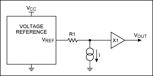
Figure 1. Adding a resistor, current source, and buffer to a voltage reference lets you adjust its output.
The buffer amplifier isolates VOUT from the load, so the only current flowing through R1 is that from the current source. As shown in Figure 2, this idea can be implemented with a highly stable voltage reference (MAX6126), a current DAC (DS4412), and a low-offset op amp (MAX9620).
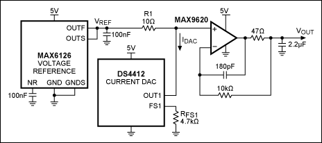
Figure 2. The MAX6126 voltage reference, the DS4412 current DAC, and MAX9620 low-offset op amp implement the idea of Figure 1.
If we choose RFS1 = 4.7kΩ, the full-scale DAC current is 0.981mA (see the DS4412 data sheet). Combined with R1 = 10Ω, this current value yields a tuning range of ±0.981mA × 10Ω = ±9.81mV, divided into 31 steps of 0.654mV each.
Depending on the performance grade of this reference and its package, the initial output accuracy can be as high as ±0.02%. The DAC's output-current accuracy is only ±6%, but the tuning range is small, so that large tolerance has only a small effect on the output error. Combining these values with a 1% resistor for R1 and the maximum offset value for the op amp yields an expression for the maximum initial output-voltage error:

For a 2.048V reference, this error is
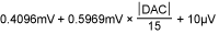
where DAC represents the DAC's decimal equivalent output value (-15 ≤ DAC ≤ +15). Thus, the maximum error introduced by the DAC is 0.5969mV, yielding a total of roughly 1mV when combined with the initial accuracy of the voltage reference itself.
Since the DAC has an operating temperature range of -40°C to +85°C, we use the voltage reference's drift specification in that same range: ±3ppm/°C. Maxim uses the box method to specify temperature drift. (See application note 4300, "Calculating the Error Budget in Precision Digital-to-Analog Converter (DAC) Applications" for details.) The maximum VREF drift is therefore
125°C × ±3ppm/°C × 2.048V = ±0.768mV.
Drift in the second term (IDAC × R1) is caused by drift in the DAC, the drift of RFS1, and the drift of R1. Drift in the DAC is specified only as a typical value of ±75ppm/°C. We assume ±25ppm/°C for the resistors. These values yield a typical drift of

Thus, the typical drift introduced by the DAC and the resistors is roughly ±0.1mV, which is substantially lower than the maximum drift of the voltage reference. The maximum input offset of the op amp over temperature is specified at 25µV, which is also much lower than the maximum drift of the voltage reference.
In a graph of output voltage as a function of the DAC code, error bars indicate the initial accuracy and temperature drift (Figure 3). Error increases slightly for the higher DAC values, mostly due to temperature drift. The measured values were recorded at room temperature and are very close to the theoretical values.
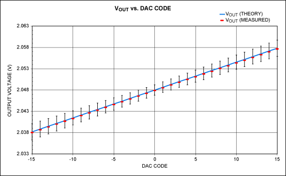
Figure 3. This graph gives the theoretical (blue line) and measured (red bars) output voltage as a function of DAC code. The nominal reference output is 2.048V. Error bars show that the accuracy drops slightly toward the absolute higher values of DAC code (error bars for the voltage meter are omitted for clarity).