Choosing the Optimal Clock Mode for MAX116xx, MAX123x, and MAX103x SAR ADCs
要約
The MAX116xx, MAX103x, and MAX123x families of low-power, multichannel, 300ksps SAR ADCs have configurable clock modes that enable flexibility when interfacing with a SPI master. This application note discusses the advantages of each clock mode and provides timing examples for each mode.
Choosing the Right Clock Mode for an Application
The MAX116xx, MAX103x, and MAX123x families of low-power, multichannel, 300ksps SAR ADCs have configurable clock modes that enable flexibility when interfacing with a SPI master. The four different clock modes allow the system designer to configure the throughput, pin count, and sample trigger. For designs with limited hardware pins available, only four lines are required to operate these ADCs in clock modes 10 and 11. For highest throughput, clock mode 11 can be used to clock the conversion as data is simultaneously read out. If precise control over the sampling instant is required, clock mode 01 provides the system designer the ability to exactly trigger each acquisition externally. For systems with additional hardware resources, clock modes 00, 01, and 10 provide a hardware indicator, active-low EOC, to signal the end of conversion. A summary of the tradeoffs of using each clock mode is shown in Table 1.
| Pin Count | Acquisition Timing | Acquisition Trigger | Averaging | Throughput | |
| Mode 00 | 5 or 6 pins | 1st Acquisition Only | Active-low CNVST | Yes | Medium |
| Mode 01 | 5 or 6 pins | Every Acquisition | Active-low CNVST | Yes | Low |
| Mode 10 | 4 or 5 pins | 1st Acquisition Only | Active-low CS | Yes | Medium |
| Mode 11 | 4 pins | Every Acquisition | SCLK | No | High |
Using Clock Mode 00
This clock mode uses five or six hardware pins and gives control over the initial acquisition timing only. In clock mode 00, acquisitions and conversions are both internally timed. After the voltage reference is chosen and the Averaging register is configured, all of the requested acquisitions and conversions across all channels can be initiated by a single active-low CNVST assert pulse. It is always best practice to clear the internal FIFO before initiating a series of conversions. To clear the FIFO without changing any of the register settings, write an input data byte of 0x18 to the device. Before initiating any conversions in clock mode 00, the conversion byte must be written before asserting active-low CNVST. Without writing the conversion byte before each series of data acquisitions/conversions, there will be no output data. This process is outlined in Figure 1.

Figure 1. Clock mode 00 flow chart.
Once the conversion byte is written, pulse active-low CNVST low for at least 40ns. Following this time period, the rising edge of active-low CNVST starts the acquisitions and conversions. Once all of the conversions are complete, the active-low EOC pin will go low, indicating the end of conversion. Since all of the acquisitions and conversions are internally timed, the time between the rising edge of active-low CNVST and falling edge of active-low EOC depends on the number of channels, scan mode, and averaging mode selected. Ensure that the master waits for active-low EOC to go low, since accessing the data before a conversion is complete can corrupt the data. However, if the total conversion time is properly calculated, a timed delay can be used following the start trigger instead of polling active-low EOC to reduce the total interface pin count.
Clock Mode 00 Example 1 – Single-Channel Conversion, No Averaging (MAX11635)
Writing the following register settings in Table 2, the MAX11635 is configured for a single conversion on channel 0 using clock mode 00, internal +2.5V reference always-on, single-ended operation, and no averaging.
| Bit 7 | Bit 6 | Bit 5 | Bit 4 | Bit 3 | Bit 2 | Bit 1 | Bit 0 | Byte | |
| Setup | 0 | 1 | CKSEL[1:0] = 00 | REFSEL[1:0] = 10 | (DIFFSEL[1:0] = 00) | 0x48 | |||
| Averaging | 0 | 0 | 1 | AVGON = 0 | NAVG[1:0] = 00 | NSCAN[1:0] = 00 | 0x20 | ||
| Conversion | 1 | X | (CHSEL2 = 0) | CHSEL[1:0] = 00 | SCAN[1:0] = 00 | X | 0x80 | ||
Since the internal reference is used and always on, assuming a low source impedance, the expected total conversion time is:
Total Conversion Time = (tACQ(max) + tCONV(max)) × nAVG × nRESULT + tRP = (1.4µs (typ) + 3.5µs (typ)) × 1 × 1 + 0 = 4.9µs (typ)
In Figure 2, active-low EOC goes low 5.2µs after the rising edge of active-low CNVST.
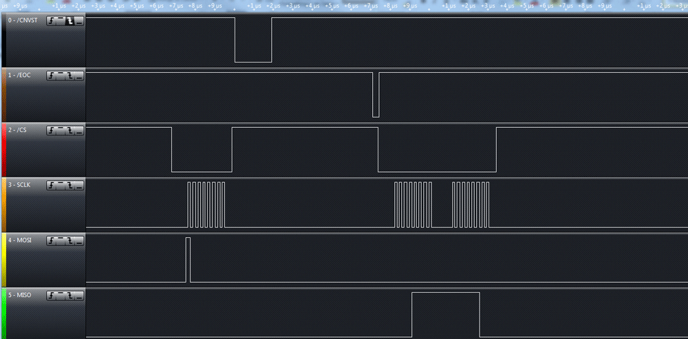
Figure 2. Mode 00 example 1 timing diagram.
Clock Mode 00 Example 2 – Four-Channel Scan, 32x Averaging (MAX11635)
Writing the following register settings in Table 3, the MAX11635 is configured to scan channel 0 through channel 3 using clock mode 00, internal +2.5V reference always-on, single-ended operation, and 32x averaging. The data returned will be the averaged result of each channel, so only four bytes are expected in the order channel 0, channel 1, channel 2, channel 3.
| Bit 7 | Bit 6 | Bit 5 | Bit 4 | Bit 3 | Bit 2 | Bit 1 | Bit 0 | Byte | |
| Setup | 0 | 1 | CKSEL[1:0] = 00 | REFSEL[1:0] = 10 | (DIFFSEL[1:0] = 00) | 0x48 | |||
| Averaging | 0 | 0 | 1 | AVGON = 1 | NAVG[1:0] = 11 | NSCAN[1:0] = 00 | 0x3C | ||
| Conversion | 1 | X | (CHSEL2 = 0) | CHSEL[1:0] = 11 | SCAN[1:0] = 00 | X | 0x98 | ||
Since the internal reference is used and always on, assuming a low source impedance, the expected total conversion time is:
Total Conversion Time = (tACQ(max) + tCONV(max)) × nAVG × nRESULT + tRP = (1.4µs (typ) + 3.5µs (typ)) × 32 × 4 + 0 = 627.2µs (typ)
In Figure 3, active-low EOC goes low 587.6?0s after the rising edge of active-low CNVST.
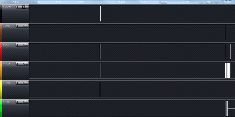
Figure 3. Mode 00 example 2 timing diagram.
Using Clock Mode 01
This clock mode uses five or six hardware pins and gives control over every single acquisition trigger. In clock mode 01, acquisitions are timed through the active-low CNVST pin and conversions are internally timed. Before initiating any conversions in clock mode 01, the conversion byte must be written before asserting active-low CNVST. For single acquisitions/conversions, this clock mode is identical to clock mode 00. However, if multiple conversions are requested, a separate active-low CNVST pulse is required to trigger each acquisition. Figure 4 summarizes the serial data flow for clock mode 01.
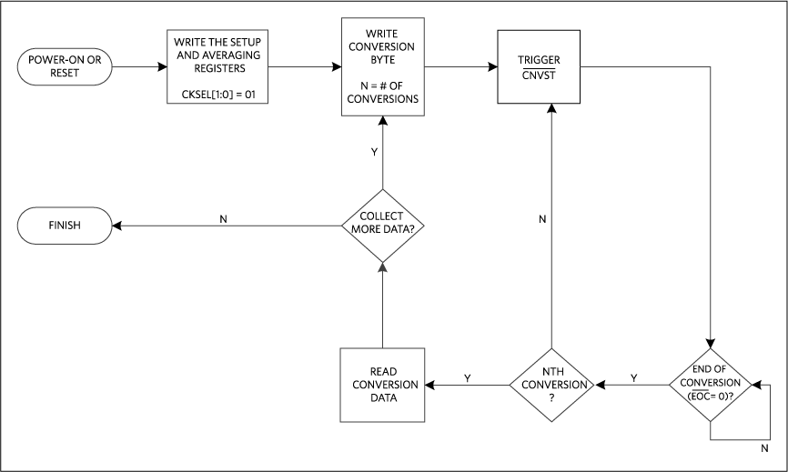
Figure 4.Clock mode 01 flow chart.
Once the conversion byte is written, pulse active-low CNVST low for at least 1.4µs. Note that this time is significantly longer than the 40ns specified for clock mode 00; please refer to the specific device data sheet for exact timing details. Following this time period, the rising edge of active-low CNVST starts the first acquisition and conversion. The active-low EOC pin will go low once each conversion is complete. If a second active-low CNVST pulse is sent before active-low EOC goes low, the output data may be corrupted. Once all of the requested conversions are complete, the active-low EOC pin will assert low and the data can be read.
Clock Mode 01 Example 1 – Single-Channel Conversion, 4x Averaging (MAX11635)
Writing the following register settings in Table 4, the MAX11635 is configured for a single-channel conversion on channel 0 using clock mode 01, internal +2.5V reference always-on, single-ended operation, with 4x averaging. Even though a single output code will be read, four active-low CNVST pulses will need to be sent to acquire the 4 samples for averaging.
| Bit 7 | Bit 6 | Bit 5 | Bit 4 | Bit 3 | Bit 2 | Bit 1 | Bit 0 | Byte | |
| Setup | 0 | 1 | CKSEL[1:0] = 01 | REFSEL[1:0] = 10 | (DIFFSEL[1:0] = 00) | 0x58 | |||
| Averaging | 0 | 0 | 1 | AVGON = 1 | NAVG[1:0] = 00 | NSCAN[1:0] = 00 | 0x30 | ||
| Conversion | 1 | X | (CHSEL2 = 0) | CHSEL[1:0] = 00 | SCAN[1:0] = 00 | X | 0x80 | ||
Since the total conversion time depends on when active-low CNVST is pulsed, there is not an exact estimate for the total time required. An example SPI transaction for clock mode 01 is shown in Figure 5.
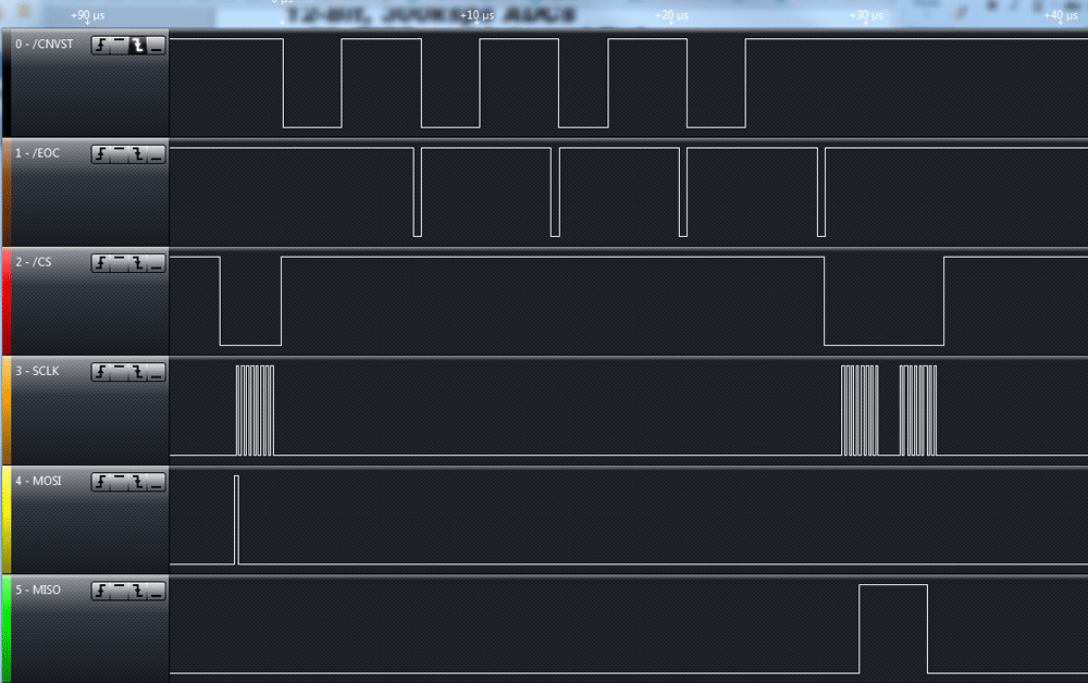
Figure 5. Mode 01 example 1 timing diagram.
Clock Mode 01 Example 2 – Four-Channel Conversion, 8x Averaging (MAX11635)
Writing the following register settings in Table 5, the MAX11635 is configured to scan channel 0 through channel 3 using clock mode 01, internal +2.5V reference always-on, single-ended operation, with 8x averaging. Sampling four channels at eight acquisitions per channel will require a total of 32 active-low CNVST pulses to complete all requested conversions. Figure 6 shows another timing example for clock mode 01 with averaging and channel scanning enabled.
| Bit 7 | Bit 6 | Bit 5 | Bit 4 | Bit 3 | Bit 2 | Bit 1 | Bit 0 | Byte | |
| Setup | 0 | 1 | CKSEL[1:0] = 01 | REFSEL[1:0] = 10 | (DIFFSEL[1:0] = 00) | 0x58 | |||
| Averaging | 0 | 0 | 1 | AVGON = 1 | NAVG[1:0] = 01 | NSCAN[1:0] = 00 | 0x34 | ||
| Conversion | 1 | X | (CHSEL2 = 0) | CHSEL[1:0] = 11 | SCAN[1:0] = 00 | X | 0x98 | ||
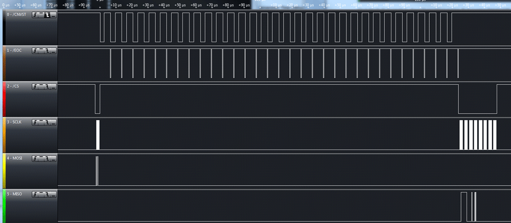
Figure 6. Mode 01 example 2 timing diagram.
Using Clock Mode 10
This clock mode uses four or five hardware pins and gives control over the initial acquisition timing only. In clock mode 10, acquisitions and conversions are both internally timed. Unlike clock mode 00, the acquisition/conversion process is initiated by the rising edge of active-low CS and not the rising edge of active-low CNVST. This mode adds the advantage of reducing the required hardware pins at the expense of exact timing control through the use of active-low CNVST. The conversion sequence starts after writing the conversion byte when active-low CS is brought high. The process for using clock mode 10 is shown in Figure 7.
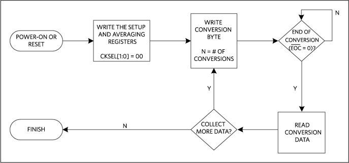
Figure 7. Clock mode 10 flow chart.
Once all of the conversions are complete, the active-low EOC pin will go low, indicating the end of conversion. Since all of the acquisitions and conversions are internally timed, the time between the rising edge of active-low CNVST and falling edge of active-low EOC depends on the number of channels and averaging selected by the conversion byte. Please refer to the device data sheet for equations to estimate the total conversion time.
Clock Mode 10 Example 1 – Four-Channel Scan, 32x Averaging (MAX11635)
Writing the following register settings in Table 6, the MAX11635 is configured to scan channel 0 through channel 3 using clock mode 10, internal +2.5V reference always-on, single-ended operation, and 32x averaging. The data returned will be the averaged result of each channel, so only four bytes are expected in the order channel 0, channel 1, channel 2, channel 3.
| Bit 7 | Bit 6 | Bit 5 | Bit 4 | Bit 3 | Bit 2 | Bit 1 | Bit 0 | Byte | |
| Setup | 0 | 1 | CKSEL[1:0] = 10 | REFSEL[1:0] = 10 | (DIFFSEL[1:0] = 00) | 0x68 | |||
| Averaging | 0 | 0 | 1 | AVGON = 1 | NAVG[1:0] = 11 | NSCAN[1:0] = 00 | 0x3C | ||
| Conversion | 1 | X | (CHSEL2 = 0) | CHSEL[1:0] = 11 | SCAN[1:0] = 00 | X | 0x98 | ||
Since the internal reference is used and always on, assuming a low source impedance, the expected total conversion time is:
Total Conversion Time = (tACQ(max) + tCONV(max)) × nAVG × nRESULT + tRP = (1.4µs (typ) + 3.5µs (typ)) × 32 × 4 + 0 = 627.2µs (typ)
In Figure 8, active-low EOC goes low 587.0µs after the rising edge of active-low CS.
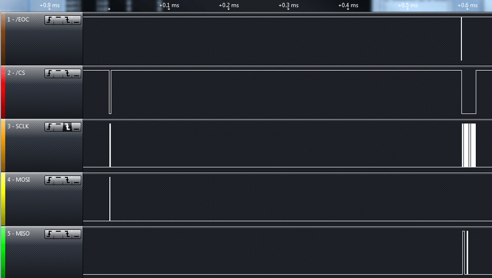
Figure 8. Mode 10 example timing diagram.
Using Clock Mode 11
This clock mode uses four hardware pins and only gives the designer control over the conversion clock rate. In clock mode 11, both acquisitions and conversions are timed externally through the SPI interface pins. Active-low CNVST and active-low EOC are unused, and both scanning and averaging are disabled in this clock mode. When writing the conversion byte, the acquisition is triggered on the SCLK falling edge immediately following the CHSEL channel select bits. The SCAN[1:0] bits in the conversion byte are unused in this clock mode, as scanning is disabled and the voltage acquisition has already started when they are clocked out. The acquisition finishes on the falling edge of the first bit of the next SPI input. This means that, if continuously clocked, three SCLK periods are used for the acquisition time. In order to satisfy the 0.6µs minimum acquisition time (longer time is required for non-zero source impedances), the maximum SCLK frequency that is used in this clock mode is 4.8MHz. Three clock cycles at this frequency take a total time of 0.625µs.
Figure 9 shows the flow required to use clock mode 11. After writing the conversion byte, the following 16 SCLK cycles are used to clock out the requested sample. The first 8 SCLK cycles immediately following a conversion byte should not be used to initiate another conversion. However, the second 8 SCLK cycles can be used to simultaneously clock out the LSB of output data and clock in the next conversion byte. Ensure that active-low CS is pulsed high for no more than 100µs between the first set 8 SCLK cycles and second set of SCLK cycles. Writing a conversion byte in every other 8-bit SPI access will yield the maximum output data rate possible in clock mode 11. Once the device is configured, active-low CS can be kept low to continuously initiate new conversions and clock out the resulting data.
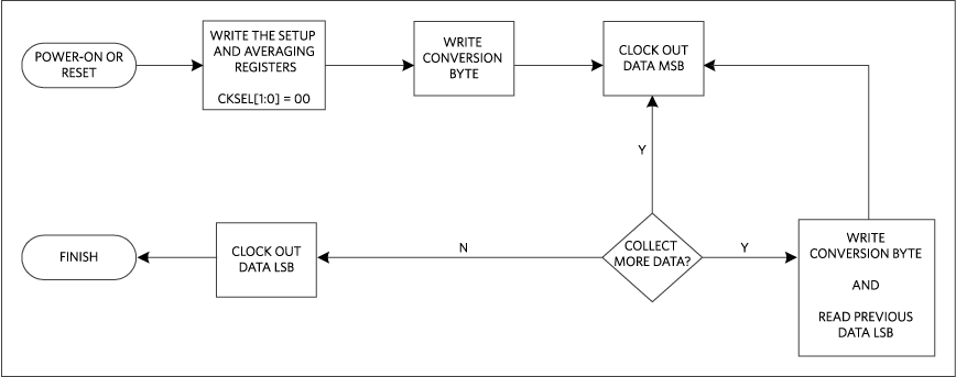
Figure 9. Clock mode 11 flow chart.
Clock Mode 11 Example 1 – Single-Channel Scan, No Averaging (MAX11635)
Writing the following register settings in Table 7, the MAX11635 is configured to scan channel 0 using clock mode 11, internal +2.5V reference always-on, single-ended operation, and no averaging (disabled by default).
| Bit 7 | Bit 6 | Bit 5 | Bit 4 | Bit 3 | Bit 2 | Bit 1 | Bit 0 | Byte | |
| Setup | 0 | 1 | CKSEL[1:0] = 11 | REFSEL[1:0] = 10 | (DIFFSEL[1:0] = 00) | 0x78 | |||
| Averaging | 0 | 0 | 1 | AVGON = 0 | NAVG[1:0] = 00 | NSCAN[1:0] = 00 | 0x20 | ||
| Conversion | 1 | X | (CHSEL2 = 0) | CHSEL[1:0] = 00 | SCAN[1:0] = 00 | X | 0x80 | ||
The total conversion time in this clock mode is directly dependent on the SCLK period. Figure 10 shows an example of the maximum output data rate by sending a conversion byte every other 8-bit SPI transaction with a SCLK frequency of 4.8MHz.
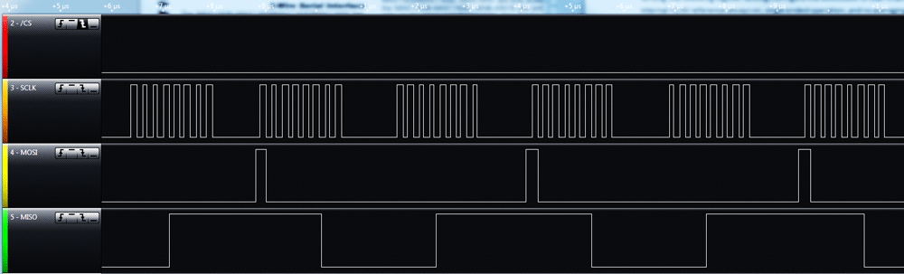
Figure 10. Mode 11 example timing diagram.
Summary
The different clock modes in the MAX116xx, MAX103x, and MAX123x families of low-power, multichannel, 300ksps SAR ADCs arm system designers with a variety of design choices when choosing the best SPI interface. Acquisition and conversion timing, hardware event triggers, pin count, and maximum throughput are all affected by the interface chosen.