Assembly Guidelines for (uSLIC) Packages
要約
This application note discusses Analog Devices’ uSLIC™ packages, and provides PCB design and board assembly process guidelines.
Introduction
The uSLIC™ package is a leadless, substrate-based open-frame package with embedded die in a substrate and passive component(s) assembled on top.
uSLIC packages have several advantages including:
- A small footprint per I/O resulting in significant PCB space savings.
- Superior electrical performance compared to side-to-side SIP packages.
- Uses standard surface mount assembly technology.

Figure 1. Package outline drawing of the uSLIC package (Specific Example (MAXM17532): A = 1.5mm ±0.15mm, A1 = 1.2mm(max), b = 0.25mm ±0.05mm, c = 0.05mm ±0.05mm, D = 3.00mm ±0.05mm, E = 2.60mm ±0.05mm, e = 0.50mm ±0.05mm, F = 2.50mm ±0.20mm, G = 2.00mm ±0.20mm, L = 0.40mm ±0.05mm).
PCB Design Guidelines
A PCB using FR-4 or BT laminate material is recommended. Common surface finish such as organic solderability preservative (OSP) and electroless nickel/immersion gold (ENIG) is recommended.
A well-designed and manufactured PCB is required for optimum manufacturing yields and product performance. For a pitch size of 0.5mm, Analog recommends the use of NSMD pads since it provides a larger metal area for the solder to anchor to the edges of the metal pads. NSMD improves the solder joint reliability. Refer to Analog’s 90-100027 for land pattern design. Moderately extending the land pattern outside the package boundary (about 0.15mm) helps to lower solder voids due to longer surface area for outgassing and inspecting solder connection between the unit and PCB; thus, extending the land pattern in this way is recommended. The SMD pattern, along with no-clean solders, could potentially cause solder beads to remain on the PCB; thus, the SMD pattern is not recommended.
For a non-SMD land pattern, the Cu trace in the SM open area should be 75µm to 100µm to avoid reduction in device standoff and should be balanced in different directions across the board to avoid device shift.
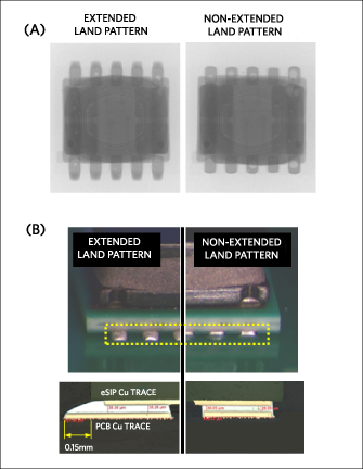
Figure 2. Recommended "extended land pattern" design shows (a) good solder voiding level and (b) is side-inspectable.
Handling
Analog doesn’t recommend manually surface mounting the device on the PCB given the size and configuration of the device. If manual handling is required, the following is recommended:
- Use a vacuum pickup hand tool with soft-tip head
- Use minimal force when picking up and placing the module. Stop about 1mm above and release the unit into its container
Stencil
The stencil thickness and pattern geometry determine the precise volume of solder paste deposited onto the device land pattern. Stencil alignment accuracy and consistent solder volume transfer is critical for uniform solder reflow.
Using a stainless steel laser-cut stencil is recommended. A square-shaped stencil opening is preferred over round-shaped openings and the corners of the square apertures can be rounded to facilitate solder release. To further improve solder release, the opening should have a larger bottom opening than the top side to form a ~5°C positive tamper. Analog recommends to use a 4mil to 5mil stencil thickness. The stencil openings designed to be within -1mil to ~+1mil (-25µm to ~+25µm) per side compared to the PCB pad size show good soldering results. The stencil aperture must meet the industry-standard area ratio of (area of aperture opening/aperture wall area) > 0.66.
SMT Assembly
Standard SMT equipment and process are used for uSLIC assembly. The process flow is the following:
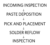
Figure 3. Recommended uSLIC assembly process.
Both solder paste or flux printing and flux dipping approaches provide acceptable assembly quality and reliability.
Solder Paste
Analog recommends using a type III or IV no-clean solder paste with an NSMD land pattern. A low-residue, no-clean solder paste (eutectic Sn63/Pb37 or lead-free SAC305 alloy SnAgCu) is commonly used. No-clean solder, however, used with PCBs with the SMD land pattern has shown solder beads in our study and is not recommended. A water-soluble paste can be used if the residue underneath the device can be adequately cleaned.
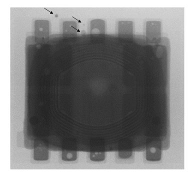
Figure 4. Solder beads (black arrows) are observed using no-clean solder on PCB using SMD land pattern.
Automated Component Pick and Place
A pick and place machine with a placement accuracy better than ±0.05mm is recommended. Conventional placement systems can be employed using either the uSLIC outline or the position of the pads as a placement guide. A placement guide using the position of the pads tends to be more accurate but slower and requires a complex vision processing system. A package outline placement method runs faster but is less accurate. The contract PCB assembler can determine the most acceptable method to employ for this process. Low mounting speed is recommended to prevent the paste from squeezing out. The following pickup and place parameters are recommended:
- The pickup area is the top of the inductor, which is 2mm x 2.5mm. The pickup location must be in the center of the inductor.
- Use 1.3mm or smaller nozzle. Picking up outside the nozzle pickup zone results in inductor crack.
- Use minimum force or no more than 3N (0.305kgf). The release force should be a part of process optimization so that the unit is pressed into the solder but does not cause solder beading or bridging issues. Too much unnecessary force also causes unit damage and should be avoided.
- When moving the unit into its container, stop at 1mm above the unit to pick up the part and release the part into the tray.
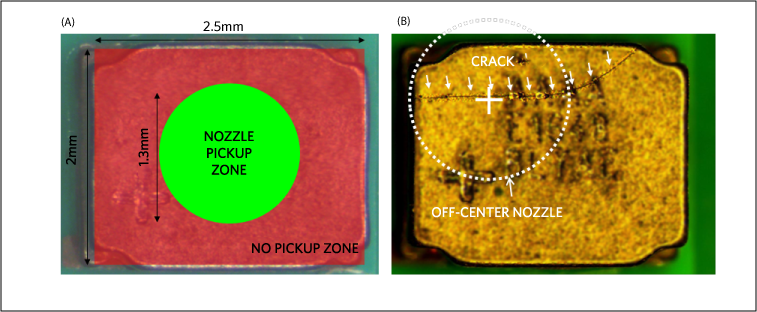
Figure 5. (a) Recommended nozzle pickup region (green circle); (b) inductor top crack could be induced by placing the nozzle outside the pickup zone (example shows using a 1.48mm diameter with the nozzle placed off-center).
Reflow Profile
Analog recommends using an 8 zone or greater oven. A nitrogen atmosphere oven is preferred since it offers better wetting properties and a reduction in solder-joint voids.
As with all surface-mount devices, it is important that the reflow profiles be optimized and tested as part of an overall process development. In addition, the profile must be checked at different locations on the board to ensure that the hottest and coldest temperature are still within recommended temperatures in the reflow profile. Component temperatures might vary due to surrounding components, locations of parts on the PCB, and package densities.
The reflow profile guidelines are based on the temperature at the actual lead to the PCB pad solder joint location. The actual temperature of the solder joint is often different than the temperature settings in the reflow system. It is important that reflow-specific profiles are completed using thermocouples at the actual solder joint locations and characterized using the reflow guidelines outlined in Figure 6 below for "lead-free" solder.
| Zone | 1 | 2 | 3 | 4 | 5 | 6 | 7 | 8 |
| Top | 89 | 142 | 180 | 201 | 259 | 253 | 201 | 139 |
| Bottom | 89 | 142 | 180 | 201 | 259 | 253 | 201 | 139 |
| Conveyor Speed (cm/min): 56.0 | ||||||||
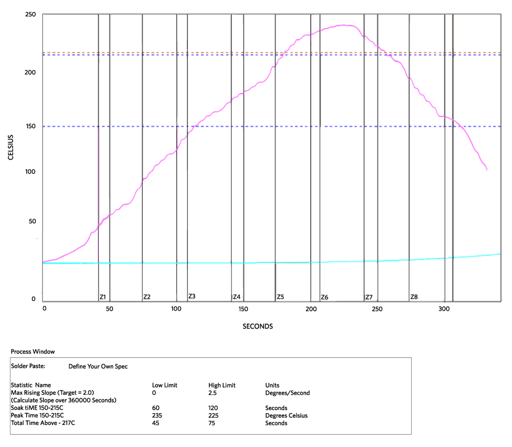
Figure 6. Recommended reflow profile for Pb-free solders per JEDEC JSTD-020.
Solder Joint Inspection
Post-reflow inspection of the uSLIC on PCBs is typically accomplished by using visual inspection plus a transmission-type x-ray. An x-ray can be used for reflow process monitoring and as a failure analysis tool. A 2-D x-ray system with oblique view at highest magnification (OVHM) is recommended since it can detect solder bridges, opens, and voids.
Moisture Sensitivity
All Analog uSLIC modules meet MSL3 standard per the JEDEC specification JSTD020D.1. Parts are shipped in tape-and-reel form. All parts are baked and dry-packed with desiccants and a humidity indicator card. If the humidity indicator card has turned pink, or if the parts have been exposed to longer than their floor life, subject the packages to bake at 125°C for 48 hours.
Rework
Refer to JEDEC specification J-STD-033C for rework of moisture and reflow sensitive surface-mount devices. Rework is recommended using an automated hot-air rework station. Localized heating is recommended to remove the uSLIC component. PCBs with uSLIC mounted are recommended to be baked at 125°C prior to rework process.
Removal of uSLIC from PCB
The bottom of the PCB should be heated using convective heaters while hot air or gas is used on the top side of the component (to prevent warpage). The nozzle should be used to direct the air to the component only, to reduce heating of adjacent components. Nozzle size should follow the pick-and-place nozzle size recommended in the "Automated Component Pick and Place" section. Excessive airflow should also be avoided. Air velocity of 15l to 20l per minute is a good starting point. Thermocouples should be used on the top and bottom sides to monitor actual temperature of the part. Maximum part temperature should be above the liquidous temperature of 217°C, but should not exceed 245°C. Once the joints have reflowed, the vacuum lift-off should be automatically engaged during the transition from reflow to cool down to remove the part.
Replacing uSLIC
A uniform and precise deposit can be achieved if a miniature stencil specific to the component is used. The stencil aperture should be aligned with the pads under 50x to 100x magnification. The stencil should then be lowered onto the PCB and the paste should be deposited with a small metal squeegee blade. Follow stencil thickness, stencil design, solder recommendations, and screen-printing guidelines as provided for original PCB assembly.
As the leads are on the underside of the package, a split-beam optical system should be used to align the component on the motherboard. The alignment should be done at 50x to 100x magnification. The placement machine should have the capability of allowing fine adjustments in X, Y, and rotational axes. Pick up the unit within the recommended pickup zone and align it on the solder paste area. Then, place the unit. The reflow profile developed during original attachment or removal should be used to attach the new component.
Shock and Vibration Data
Mechanical Shock
Standard: JESD22-B111 and JESD22-B104 Condition-B
Test Condition:
Peak Level – 1500G (half-sine waveform)
Duration – 0.5ms
Vibration
Standard: JESD22-B103, Condition-3
Test Condition:
Peak acceleration – 3G
Displacement peak-to-peak – 0.75mm
Cross-over frequency – 45Hz
Min. frequency – 5Hz
Max. frequency – 500Hz