目的
発振器の機能は、様々な回路構成によって実現できます。その中から、本稿ではハートレー発振器を取り上げることにします。その回路では、タップを備えるインダクタを分圧器として使用することでフィードバック経路を実現します。
背景
ハートレー発振器は優れた回路です。歪みが比較的小さい30kHz~30MHzの正弦波信号を生成したい場合には特に有用です。ハートレー発振器は様々な構成で実現されますが、通常は1つの大きな特徴を備えています。それは、タップを備えるインダクタを分圧器として使用するというものです。図1に示した一般的なハートレー発振器では、インダクタL1、L2が分圧器として機能します。図1の回路の発振周波数は、任意の並列共振回路と同様に以下の式で計算できます。

ここで、L = L1 + L2です。
図1の回路において、発振周波数を決定する並列共振同調回路はL1、L2とコンデンサC1で構成されています。この同調回路は、ベース接地アンプ(ベース共通アンプ)の構成要素であるNPNトランジスタQ1のコレクタの負荷インピーダンスとなります。このように回路を構成することにより、ベース接地アンプのゲインは共振周波数においてのみ高くなります。Q1のベースは、抵抗R1とR2から成る抵抗分圧器によって適切なDCレベルにバイアスされています。また、Q1のベースとACグラウンドの間にはコンデンサC3が配置されています。これは、Q1のベース用のデカップリング・コンデンサです。ベース接地モードでは、エミッタへの入力信号とコレクタに現れる出力電圧信号が同位相になります。このような構成により、コレクタの同調負荷から(L1とL2の間のノードから)カップリング・コンデンサC2を介してエミッタまで、出力信号の一部が確実にフィードバックされます。つまり、発振に必要な正のフィードバックが得られるということです。


また、C2とエミッタ抵抗R3によって時定数が決まります。それにより、Q1のエミッタに対してフィードバック信号の振幅に比例する平均DC電圧レベルが提供されます。その結果、クローズド・ループ・ゲインがこの発振器に必要な値である1になるようアンプのゲインが自動的に制御されます。エミッタのノードはベース接地アンプの入力として使用されるので、R3はデカップリングされていません。一方、ベースとACグラウンドの間にC3が配置されていることから、発振周波数におけるリアクタンスは非常に小さな値になります。
事前のシミュレーション
実習に進む前に、図1のハートレー発振器のシミュレーションを実施しておくとよいでしょう。そのためには、まず図1のとおりにシミュレーション用の回路図を作成します。ここでは、R3を1kΩ、Q1のコレクタ電流を約1mAとしてR1とR2の値を計算してください。回路で使用する電源電圧は10Vに設定することにします。抵抗分圧器に定常的に流れる電流の量を少なく抑えるために、R1とR2の値の和ができるだけ大きくなるようにしましょう(例えば、10kΩ以上)。出力用のACカップリング・コンデンサであるC4とC3の値は0.1μFに設定します。このシミュレーションと実習では、タップを備えるインダクタの代わりに2個のインダクタL1とL2を使用することにします。C1の値については、L1が1μH、L2が10μHの場合の共振周波数が750kHzに近い値になるように選択してください。以上でシミュレーション用の回路図が完成しました。この回路を対象としてトランジェント・シミュレーションを実行してください。得られた結果は、必ず保存しておきましょう。その結果と実際の回路で収集した測定結果を比較する形で実習レポートを作成してください。
準備するもの
- アクティブ・ラーニング・モジュール「ADALM2000」
- ソルダーレス・ブレッドボード
- ジャンパ線キット
- NPNトランジスタ:「2N3904」(1個)
- インダクタ:1μH(1個)、10μH(1個)、100μH(1個)
- コンデンサ:1nF(1個。C1の値を変更するために使用)、0.1nF(2個。「104」とマーキングされているもの)、0.01nF(2個。「103」とマーキングされているもの)
- 抵抗:1kΩ(1個)
- その他の抵抗とコンデンサ(必要に応じて用意)
説明
図2に示すハートレー発振器の回路を、ソルダーレス・ブレッドボード上に実装します。1kΩのエミッタ抵抗であるR3により、Q1のコレクタ電流が約1mAになります。バイアス用の抵抗であるR1、R2の値は、アナログ・パーツ・キット「ADALP2000」に含まれるものを使用できるように設定してください。発振周波数は、L1、L2、C1として選択した値に応じ、約500kHz~2MHzになります。ここでは、まずL1を10μH、L2を100μHに設定します。その結果、C1の値によって決まる周波数で発振が起こります。そして10Vp-pを超える正弦波信号が出力されます。C1を様々な値に変更し、回路の動作を確認してください。その後、L1を1μH、L2を10μHに変更して同様の実験を行ってみてください。


ハードウェアの設定
図2の青色のボックスは、ADALM2000のオシロスコープのチャンネルと電源を接続する個所を表しています。電源を投入する前に、必ず配線の再確認を行ってください。図2の回路を実装したブレッドボードを図3に示します。


手順
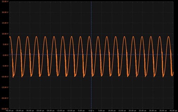
実装した回路に、5Vと-5Vの電源電圧を印加してください。その状態でオシロスコープのチャンネル1(1+)を出力端子に接続し、回路が適切に発振しているか否かを確認します。実は、R3の値の調整は容易ではありません。少しの差によって、かなり歪んだ大きな波形が生成されたり、小さい出力が断続的に生成されたり、出力が得られない状態になったりする可能性があります。R3の最適な値を見いだすためには、1kΩの抵抗をポテンショメータに置き換えて実験を行うとよいでしょう。それにより、最もきれいな波形、信頼性の高い振幅が得られる値を探し出すことができます。図4に、出力信号の波形の例を示しました。このプロットは、R1= 10kΩ、R2 = 1kΩ、R3 = 100Ω、C1 = 4.7nFの条件で取得しました。

問題1
ハートレー発振器の主機能について説明してください。
問題2
ハートレー発振器の実用的なアプリケーションとしてはどのようなものがありますか。
答えはStudentZoneで確認できます。
