Extended Reality Solution for Edge Devices

Extended Reality (XR) Solution for Edge Devices
Extended Reality (XR)* Devices are the gatekeepers between the physical and digital worlds. With one foot in the local network and one foot in the cloud, XR devices at the edge are essential hardware for enabling the next evolution of today’s internet: the metaverse.
The metaverse has the capability to take users beyond 2D browsing, delivering immersive experiences in gaming, healthcare, education, commerce, and industrial applications.
* XR is a catch-all term for the different yet related technologies (and Acronyms) which include virtual reality (VR), augmented reality (AR), and mixed reality (MR).
Value and Benefits
Intelligent edge devices are the portal to the metaverse. Building the metaverse will require a combination of superior hardware and systems that go beyond the architectures and inner workings of devices used today. We provide a portfolio of leading-edge biosensors, haptics, technologies to support functions like 3D sensing and immersive audio, and power parts ideal for XR devices.
Our technologies for edge devices include:
• Wearable Vital Signs Monitoring
• Battery Management
• Audio Solutions
• Human Machine Interface


Support 3D sensing
Monitor wearable vital signs
Support immersive audio
Signal Chains
(1)
Interactive Signal Chains

Click on the part for more details

Time of Flight Products
ADSD3030
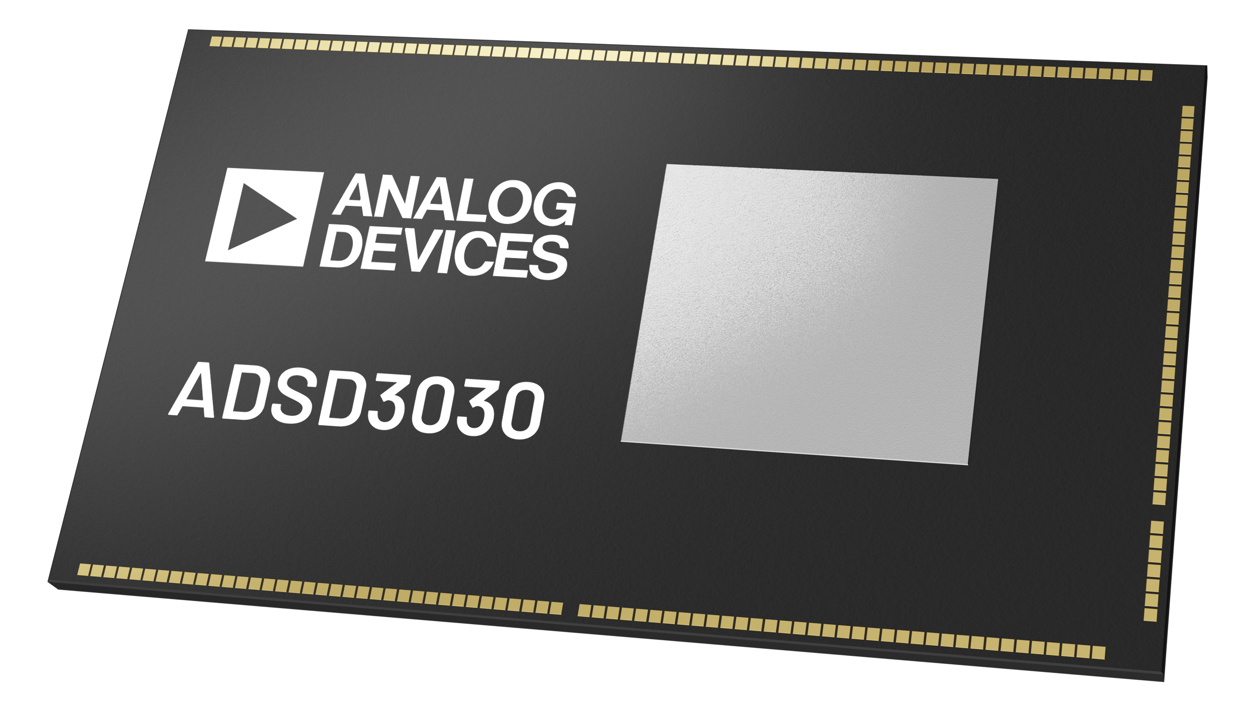
The ADSD3030 is a CMOS 3D Time of Flight (ToF)-based 3D depth and 2D visual light imager that is available for integration into 3D sensor systems. The functional blocks required for read out, which include analog-to-digital converters (ADCs), amplifiers, pixel biasing circuitry, and sensor control logic, are built into the chip to enable a cost-effective and simple implementation into systems.
The ADSD3030 interfaces electrically to a host system over a mobile industry processor interface (MIPI), Camera Serial Interface 2 (CSI-2) interface. A lens plus optical band-pass filter for the imager and an infrared light source plus an associated driver are required to complete the working subsystem.
APPLICATIONS
- Smartphones
- Augmented reality (AR) and virtual reality (VR)
- Machine vision systems (logistics and inventory)
- Robotics (consumer and industrial)
Applications
Intelligent Building Solutions
- Automatic Identification and Data Capture (AIDC) Solutions
- Surveillance Camera Solutions
Instrumentation and Measurement Solutions
- Precision Measurement Solutions
Industrial Automation
- Industrial Robotics Solutions
Healthcare Solutions
- Activity Tracking and Fall Detection Solutions
Consumer Technology Solutions
- Personal Electronics Solutions
- Home Theater and Gaming Solutions
ADSD3100
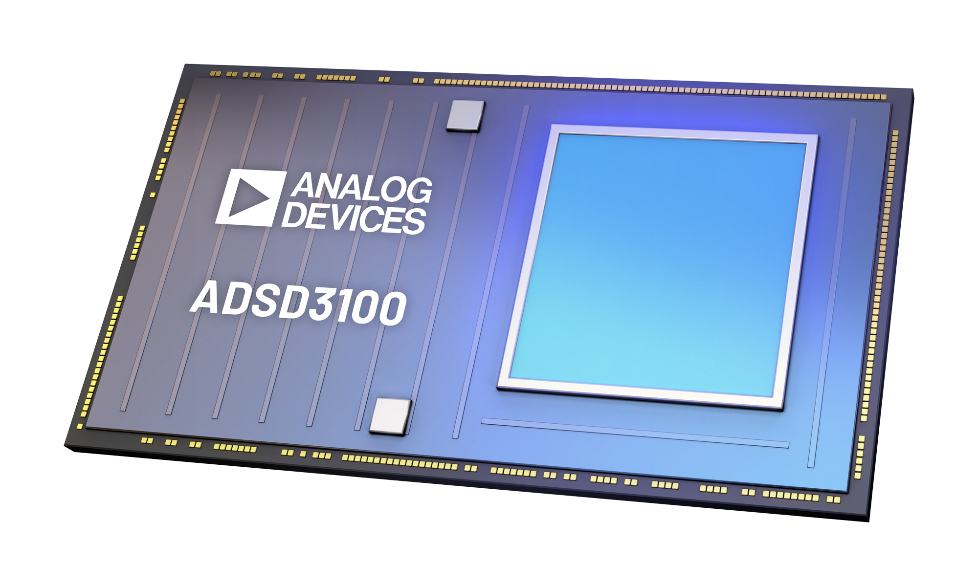
The ADSD3100 is a CMOS 3D Time of Flight (ToF)-based 3D depth and 2D visual light imager that is available for integration into 3D sensor systems. The functional blocks required for read out, which include an analog to digital converter (ADC), pixel biasing circuitry, and sensor control logic, are built into the chip to enable a cost effective and simple implementation into systems.
The ADSD3100 interfaces electrically to a host system over a mobile industry processor interface (MIPI), Camera Serial Interface 2 (CSI-2) interface. A lens plus optical band-pass filter for the imager and an infrared light source plus an associated driver are required to complete the working subsystem.
APPLICATIONS
- Smartphones
- Augmented reality (AR)/virtual reality (VR)
- Machine vision systems (logistics and inventory)
- Robotics (consumer and industrial)
Applications
Intelligent Building Solutions
- Automatic Identification and Data Capture (AIDC) Solutions
Consumer Technology Solutions
- Home Theater and Gaming Solutions
- Personal Electronics Solutions
- Extended Reality (XR) Solution for Edge Devices
Industrial Vision Technology
- 3D Time of Flight (ToF)
ADSD3500
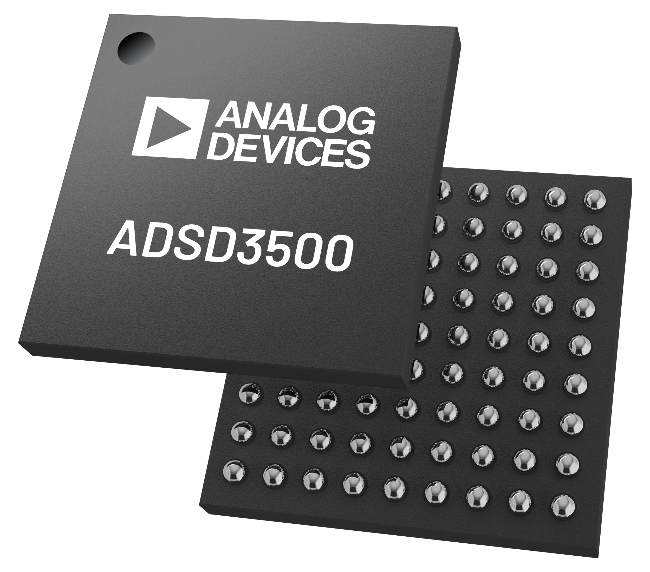
The ADSD3500 is a Time-of-Flight (ToF) Depth Image Signal Processor (ISP) for Analog Devices ToF products such as the ADTF3175 and ADSD3030. The Depth ISP processes the raw phase frames from the ToF imager, generating the final radial depth, active brightness (AB), and confidence frames. The ADSD3500 supports full computation of depth, active brightness and confidence data for 640x480 resolution, and partial depth computation (pre-phase unwrap) for 1024x1024 resolution. Data and processing flow is controlled using the integrated ARM® Cortex®-M33. Computation is performed using dedicated hardware and memory, enabling a low power ToF depth ISP solution. The ADSD3500 also controls the boot-up of the image sensor module, loading of calibration data, and triggering of frames.
The image data receiver (Rx) and transmitter (Tx) ports use standard Mobile Industry Processor Interface (MIPI) Camera Serial Link 2 (CSI-2) interfaces. Processor programming and operation are controlled through 4-wire QSPI, I2C, and I3C serial interfaces.
The ADSD3500 is available in a 3.47mm x 3.47mm WLCSP, and is specified over an operating temperature range of -25°C to +85°C.
APPLICATIONS
- Augmented reality (AR) systems
- Robotics
- Building automation
- Machine vision systems
Applications
Intelligent Building Solutions
- Automatic Identification and Data Capture (AIDC) Solutions
- Smart Building Automation Systems
- Building Automation Controllers and Network Solutions
- Building Fire Safety and Surveillance Solutions
- Smart Building Sustainability Solutions
Consumer Technology Solutions
- Home Theater and Gaming Solutions
Healthcare Solutions
- Activity Tracking and Fall Detection Solutions
Industrial Automation
- Industrial Robotics Solutions
- Intelligent Motion Control Solutions
Instrumentation and Measurement Solutions
- Automated Test Equipment
- Analytical Instruments
- Electronic Test and Measurement Solutions
- Parametric Measurement Solutions
Industrial Vision Technology
ADTF3175
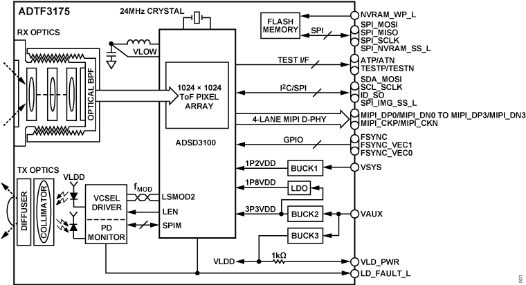
The ADTF3175 is a complete Time-of-Flight (ToF) module for high resolution 3D depth sensing and vision systems. Based on the ADSD3100, a 1 Megapixel CMOS indirect Time-of-Flight (iToF) imager, the ADTF3175 also integrates the lens and optical bandpass filter for the imager, an infrared illumination source containing optics, laser diode, laser diode driver and photodetector, a flash memory, and power regulators to generate local supply voltages. The module is fully calibrated at multiple range and resolution modes. To complete the depth sensing system, the raw image data from the ADTF3175 is processed externally by the host system processor or depth ISP.
The ADTF3175 image data output interfaces electrically to the host system over a 4-lane mobile industry processor interface (MIPI), Camera Serial Interface 2 (CSI-2) Tx interface. The module programming and operation are controlled through 4-wire SPI and I2C serial interfaces.
The ADTF3175 has module dimensions of 42mm × 31mm × 15.1mm, and is specified over an operating temperature range of -20°C to 65°C.
APPLICATIONS
- Machine vision systems
- Robotics
- Building automation
- Augmented reality (AR) systems
Applications
Intelligent Building Solutions
- Automatic Identification and Data Capture (AIDC) Solutions
- Building Fire Safety and Surveillance Solutions
Consumer Technology Solutions
- Home Theater and Gaming Solutions
- Personal Electronics Solutions
Healthcare Solutions
- Activity Tracking and Fall Detection Solutions
- Body Composition, Hydration, and Bioimpedance Analysis Solutions
Industrial Automation
- Industrial Robotics Solutions
Instrumentation and Measurement Solutions
- Electronic Test and Measurement Solutions
- Precision Measurement Solutions
Industrial Vision Technology
Vital Signs Monitoring Products
MAX30208
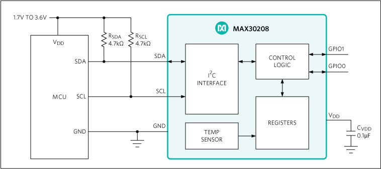
The MAX30208 operates from a 1.7V to 3.6V supply voltage, and is a low-power, high-accuracy digital temperature sensor with ±0.1°C accuracy from +30°C to +50°C and ±0.15°C accuracy from 0°C to +70° C. The MAX30208 has 16-bit resolution (0.005°C).
The device uses a standard I2C serial interface to communicate with a host controller. Two GPIO pins are available. GPIO1 can be configured to trigger a temperature conversion, while GPIO0 can be configured to generate an interrupt for selectable status bits.
The MAX30208 includes a 32-word FIFO for the temperature data and also includes high and low threshold digital temperature alarms. The device is available in a 2mm x 2mm x 0.75mm, 10-pin Thin LGA package.
Applications
- Internet of Things (IoT) Sensors
- Medical Thermometers
- Wearable Body Temperature Monitors
Applications
Consumer Technology Solutions
- Hearable and Wearable Solutions
- Wearable Vital Signs Monitoring Solutions
- Extended Reality (XR) Solution for Edge Devices
Healthcare Solutions
- Activity Tracking and Fall Detection Solutions
- Respiration Rate Measurement Solutions
- Electrocardiogram (ECG) Measurement Solutions
- Wearable Health Monitor Solutions
- Continuous Glucose Monitor (CGM) Solutions
- Diabetes Monitoring and Diagnostic Solutions
- Body Temperature Measurement Solutions
MAX32664
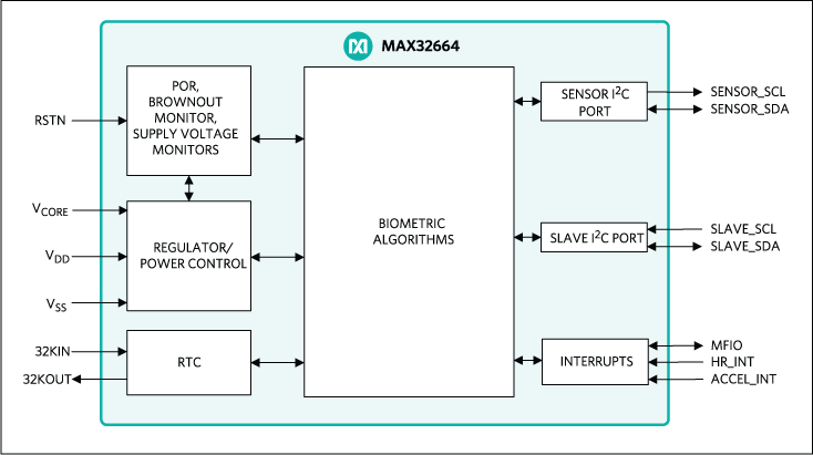
The MAX32664 is a sensor hub family with embedded firmware and world-class algorithms for wearables. It seamlessly enables customer-desired sensor functionality, including communication with Analog Devices' optical sensor solutions and delivering raw or calculated data to the outside world. This is achieved while keeping overall system power consumption in check. The device family interfaces to a microcontroller host through a fast-mode slave I2C interface for access to raw and processed sensor data as well as field updates. A firmware bootloader is also provided.
The MAX32664 Version A supports the MAX30101/MAX30102 high-sensitivity pulse oximeter and heart-rate sensor for wearable health for finger-based applications. A master mode I2C interface for communication with sensors is provided.
The MAX32664 Version B supports the MAX86140/MAX86141 for wrist-based applications. A master mode SPI interface for communication with sensors is provided.
The MAX32664 Version C supports the MAX86140/MAX86141 for wrist-based applications and MAXM86161 for ear-based applications. The device provides either a master mode SPI or an I2C interface for communication with sensors.
The MAX32664Version D supports the MAX30101/MAX30102 high-sensitivity pulse oximeter and heart-rate sensor for wearable health for finger-based applications. A master mode I2C interface for communication with sensors is provided. Version D also supports estimated blood pressure monitoring.
The wearable algorithms in the MAX32664 sensor hub support a directly connected accelerometer. They also allow feeding of X, Y, and Z samples from a host-connected accelerometer. This architecture provides robust detection and compensation of motion artifacts in captured samples.
The tiny form factor 1.6mm x 1.6mm WLP or 3mm x 3mm TQFN allows for integration into extremely small application devices.
Applications
- Wearable Fitness
- Hearables
- Wearable Medical
- Portable Medical
- Mobile Devices
Applications
Consumer Technology Solutions
- Hearable and Wearable Solutions
- Wearable Vital Signs Monitoring Solutions
- Extended Reality (XR) Solution for Edge Devices
Healthcare Solutions
- Activity Tracking and Fall Detection Solutions
- Respiration Rate Measurement Solutions
- Electrocardiogram (ECG) Measurement Solutions
- Wearable Health Monitor Solutions
- Oxygen Saturation (SpO2) Measurement Solutions
MAX86178

The MAX86178 is a highly integrated, multiple vital-sign monitoring device with a complete photoplethysmogram (PPG), electrocardiogram (ECG) and biopotential (BioZ) analog front end (AFE) for wearable applications. The MAX86178 offers high performance for wellness and clinical applications with low power for long battery life.
The PPG data acquisition system supports up to 6 LEDs and 4 photodiode inputs. The LEDs are programmable from two high-current, 8-bit LED drivers. The receive path has two low-noise, high-resolution readout channels that each include independent 20-bit ADCs and industry-leading ambient light cancellation (ALC) circuits, producing the highest performing integrated optical data acquisition system on the market today.
The ECG channel has EMI filtering, internal lead biasing, right-leg drive, and extensive calibration voltages for built-in self-test. The ECG channel also has high-input impedance, low noise, high CMRR, programmable gain, an anti-aliasing low-pass filter, and a high-resolution ADC. It is designed to meet IEC 60601-2-47 Ambulatory ECG Systems monitoring compliance requirements.
The BioZ receive channel has EMI filtering and extensive calibration features. The BioZ receive channel also has high input impedance, low noise, programmable gain, low-pass and high-pass filter options, and a high-resolution ADC. There are several modes for generating input stimulus: balanced square-wave source/sink current, sine-wave current, and both sine-wave and square-wave voltage stimuli. A wide range of stimulus magnitudes and frequencies is available.
The MAX86178 has DC and AC lead-off detection, a flexible timing system, and a PLL. All three sensor channels are synchronized. The MAX86178 is available in a 7 x 7 49-bump wafer-level package (WLP) with package dimensions of 2.77mm x 2.57mm, and operates over -40°C to +85°C temperature range.
Applications
- Ambulatory Heart Monitors
- Impedance Cardiography/Hemodynamic Monitors
- Pulse Arrival Time (PAT), Pulse Travel Time (PTT), Pulse Wave Velocity (PWV) Assessments
- Pulse-Oximetry Devices
- Single- and Multi-Frequency Bioimpedance Analysis
- Smart-Clothing Applications
- Wearable Vital-Sign Monitors
Applications
Healthcare Solutions
- Activity Tracking and Fall Detection Solutions
- Respiration Rate Measurement Solutions
- Electrocardiogram (ECG) Measurement Solutions
- Wearable Health Monitor Solutions
- Continuous Glucose Monitor (CGM) Solutions
- Diabetes Monitoring and Diagnostic Solutions
- Body Composition, Hydration, and Bioimpedance Analysis Solutions
- Non-Invasive Blood Pressure (NIBP) Solutions
- Oxygen Saturation (SpO2) Measurement Solutions
Consumer Technology Solutions
- Wearable Vital Signs Monitoring Solutions
- Extended Reality (XR) Solution for Edge Devices
Battery Management Products
MAX17332

The MAX17332 is a 35μA IQ stand-alone charger, fuel gauge, protector, and battery internal self-discharge detection IC for 1-cell lithium-ion/polymer batteries. When a voltage source is present, the IC regulates charging by modulating the charge N-FET, using AccuCharge™charger technology. The IC regulates charge voltage, current, and FET temperature. Stand-alone charging is supported by flexible configuration in nonvolatile memory. The IC supports the following applications:
- Low-Power Charging
- 1mA to 500mA directly from universal 5V USB
- No USB identification/coordination needed
- High-Power Parallel Packs (>1000mA)
- Independently charges parallel packs
- Prevents cross-charging for parallel batteries
- Coordinates external DC-DC with alerts
- Minimizes dropout and heat
- Protection and Charging Control—pack or host side
The IC ideal diode circuit supports a quick response to system transients and adapter removal with low voltage drop across the CHG FET.
The IC uses the ModelGauge™ m5 EZ algorithm that combines the short-term accuracy and linearity of a coulomb counter with the long-term stability of a voltage-based fuel gauge to provide industry-leading accuracy. The IC automatically compensates for cell aging, temperature, and discharge rate while providing accurate state-of-charge (SOC) in milliampere-hours (mAh) or percentage (%) over a wide range of operating conditions.
The IC monitors the voltage, current, temperature, and state of the battery to provide protection against over/undervoltage, overcurrent, short-circuit, over/undertemperature and overcharge conditions, and internal self-discharge protection using external high-side N-FETs to ensure that the lithium-ion/polymer battery operates under safe conditions which prolongs the life of the battery.
APPLICATIONS
- USB PPS and Direct Charging
- Smart Batteries and Hybrid Supercap Batteries
- Dual Screen Smartphones, Tablets
- Hearables, Wearables, Smartwatches
- Medical Devices, Health, Fitness Monitors
- Handheld Radios, Computers, Accessories
- Home/Building Automation, Sensors, Cameras
- Parallel Battery AR/VR Systems
Applications
Consumer Technology Solutions
- Personal Electronics Solutions
- Ultra Low Power (ULP), Space-Saving Power and Battery Management Solutions
- Hearable and Wearable Solutions
MAX20303
The MAX20303 is a highly integrated and programmable power management solution designed for ultra-low-power wearable applications. It is optimized for size and efficiency to enhance the value of the end product by extending battery life and shrinking the overall solution size. A flexible set of power-optimized voltage regulators, including multiple bucks, boost, buck-boost, and linear regulators, provides a high level of integration and the ability to create a fully optimized power architecture. The quiescent current of each regulator is specifically suited for 1µA (typ) to extend battery life in always-on applications.
The MAX20303 includes a complete battery management solution with battery seal, charger, power path, and fuel gauge. Both thermal management and input protection are built into the charger.
The device also includes a factory programmable button controller with multiple inputs that are customizable to fit specific product UX requirements.
Three integrated LED current sinks are included for indicator or backlighting functions, and an ERM/LRA driver with automatic resonance tracking is capable of providing sophisticated haptic feedback to the user.
The device is configurable through an I2C interface that allows for programming various functions and reading device status, including the ability to read temperature and supply voltages with the integrated ADC.
This device is available in a 56-bump, 0.5mm pitch 3.71mm x 4.21mm, wafer-level package (WLP) and operates over the -40°C to +85°C extended temperature range.
Applications
- IoT
- Wearable Devices
Applications
Consumer Technology Solutions
- Extended Reality (XR) Solution for Edge Devices
MAX20360
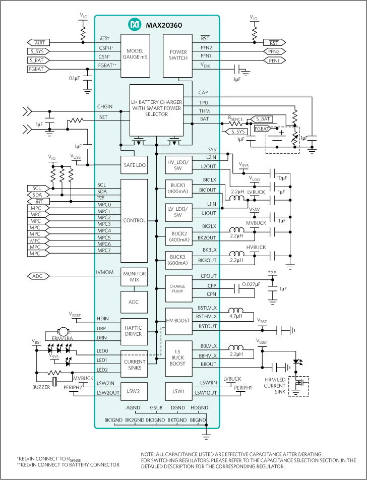
The MAX20360 is a highly integrated and programmable power management solution designed for ultra-low-power wearable applications. It is optimized for size and efficiency to enhance the value of the end product by extending battery life and shrinking the overall solution size. A flexible set of power-optimized voltage regulators, including multiple buck, boost and buck-boost converters, and linear regulators, provides a high level of integration and the ability to create a fully optimized power architecture. The quiescent current of each regulator is ultra-low targeted at extending battery life in always-on applications.
The MAX20360 includes a complete battery management solution with battery seal, charger, power path, and fuel gauge. Both thermal management and input protection are built into the charger. The device also includes a factory programmable button controller with multiple inputs that are customizable to fit specific product UX requirements. Three integrated LED current sinks are included for indicator or backlighting functions, and an ERM/LRA driver with automatic resonance tracking is capable of providing sophisticated haptic feedback to the user. A low noise, 1.5W buck-boost converter provides a clean way to power LEDs commonly used in optical heart-rate systems. The device is configurable through an I2C interface that allows for programming various functions and reading the device status, including the ability to read temperature and supply voltages with the integrated ADC. This device is available in a 72-bump, 0.5mm pitch, 4.88mm x 4.19mm, wafer-level package (WLP) and operates over the -40°C to +85°C extended temperature range.Applications
- Wearable Devices
- IoT
Applications
Healthcare Solutions
- Activity Tracking and Fall Detection Solutions
- Respiration Rate Measurement Solutions
- Electrocardiogram (ECG) Measurement Solutions
- Wearable Health Monitor Solutions
- Insulin Pump Solutions
- Diabetes Monitoring and Diagnostic Solutions
- Continuous Glucose Monitor (CGM) Solutions
Consumer Technology Solutions
- Power and Battery Management Solutions for Hearables and Wearables
- Extended Reality (XR) Solution for Edge Devices
MAX77714

The MAX77714 is a complete power-management IC (PMIC) for portable devices using System-on-Chip (SoC) applications processors.
Two 2A (SD2/3), one 3A (SD1), and one 4A (SD0) stepdown regulator switch at 2MHz, allowing the use of small magnetic components. The output voltages for SD0 and SD1 are programmable from 0.26V to 1.52V in 10mV steps. The output voltage for SD2 is programmable from 0.6V to 2.194V in 6.5mV steps. The output voltage for SD3 is programmable from 0.6V to 3.78V in 12.5mV steps.
Nine low-dropout (LDO) linear regulators supply power to various system blocks. Each LDO features a programmable active-discharge circuit in shutdown. All LDOs feature two soft-start rates to limit inrush current during start up.
Eight programmable GPIOs can be programmed as general purpose inputs (GPI), general purpose outputs (GPO), or alternate modes for additional functionalities.
The real-time clock (RTC) with an external crystal oscillator provides time keeping and alarm wake-up functions. An internal silicon oscillator is available for systems that do not want to use the crystal oscillator. In addition, a watchdog timer is integrated for system monitoring purposes.
An integrated ON/OFF controller, in combination with flexible power sequencer (FPS), provides maximum flexibility in setting power-up/down sequences with minimal intervention from the applications processor.
The 70-bump, 4.1mm x 3.25mm x 0.7mm, 0.4mm pitch wafer-level package (WLP) is ideal for space constrained applications.
Factory-programmable options allow the MAX77714 to be tailored for many applications. Contact the factory for more information about programmable options; minimum order quantities may apply.
![]() Design Solution: Power Your Computationally Intensive Application Processor with a Single PMIC ›
Design Solution: Power Your Computationally Intensive Application Processor with a Single PMIC ›
Applications
- AR/VR Headsets
- Automotive Aftermarket Accessories
- Digital Cameras
- Drones
- Handheld Gaming Devices
- Home Automation Hubs
- Smartphones/Tablet PCs
- Streaming Devices/Set-Top Boxes
Applications
Consumer Technology Solutions
- Extended Reality (XR) Solution for Edge Devices
Audio Products
MAX98304
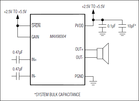
The MAX98304 mono 3.2W Class D amplifier provides Class AB audio performance with Class D efficiency. This device offers five selectable gain settings (0dB, 3dB, 6dB, 9dB, and 12dB) set by a single gain-select input (GAIN).
Active emissions-limiting, edge-rate, and overshoot control circuitry greatly reduces EMI. A filterless spread-spectrum modulation scheme eliminates the need for output filtering found in traditional Class D devices. These features reduce application component count.
The IC's 0.95mA at 3.7V (1.2mA at 5V) quiescent current extends battery life in portable applications.
The IC is available in a 9-bump (1.0mm x 1.0mm) WLP with 0.3mm pitch that is specified over the extended -40°C to +85°C temperature range.
Applications
- Cellular Phones
- MP3 Players
- Notebook and Netbook Computers
- Portable Audio Players
- Tablets
- VoIP Phones
Applications
Consumer Technology Solutions
- Extended Reality (XR) Solution for Edge Devices
MAX98360A/B/C/D
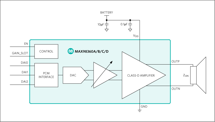
The MAX98360A/B/C/D is an easy-to-use, low-cost, digital pulse-code modulation (PCM) input Class-D amplifier that provides industry-leading, Class-AB audio performance with Class-D efficiency. The digital audio interface automatically recognizes different PCM and TDM clocking schemes which eliminates the need for I2C programming. Simply supply power, LRCLK, BCLK, and digital audio to generate audio. Furthermore, a novel pinout allows customers to use the cost-effective WLP package with no need for expensive vias.
The digital audio interface is highly flexible. The devices support I2S, left-justified, and 8-channel time division multiplexed (TDM) data formats. The digital audio interface accepts 8kHz, 16kHz, 32kHz, 44.1kHz, 48kHz, 88.2kHz, and 96kHz sample rates. Data words can be 16-bit, 24-bit, or 32-bit in I2S and left-justified modes and 16-bit or 32-bit in TDM mode.
Digital audio interface input thresholds are ideal for interfacing to 1.2V and 1.8V logic. The devices can tolerate logic input voltages up to 5.5V.
The MAX98360A and MAX98360B have fast 1ms turn-on times while the MAX98360C and MAX98360D ramp the volume over 13ms during turn-on and turn-off.
The devices eliminate the need for the external MCLK signal that is typically used for PCM communication. This reduces EMI and possible board coupling issues in addition to reducing the size and pin count. The devices also feature a very high wideband jitter tolerance (12ns, typ) on BCLK and LRCLK to provide robust operation.
Active emissions-limiting, edge-rate limiting, and overshoot control circuitry greatly reduce EMI. A filterless spread-spectrum modulation scheme eliminates the need for output filtering found in traditional Class-D devices and reduces the component count of the solution.
The devices are specified over the -40°C to +85°C temperature range.
MAX98360 Version Management
| Ramping | Frame Sync Pulse on LRCLK | 50% Duty Cycle on LRCLK | ||||
|---|---|---|---|---|---|---|
| Turn-On/Off Ramp | Start-Up Time | Format | BCLK Active Edge | Format | BCLK Active Edge | |
| MAX98360A | Ramp Disabled | 1ms | TDM | rising | I2S | rising |
| MAX98360B | Ramp Disabled | 1ms | TDM | falling | LJ | rising |
| MAX98360C | Ramp Enabled | 13ms | TDM | rising | I2S | rising |
| MAX98360D | Ramp Enabled | 13ms | TDM | falling | LJ | rising |
Applications
- Single Li-ion Cell/5V Devices
- Smart Speakers
- Notebook Computers
- IoT Devices
- Gaming Devices (Audio and Haptics)
- Smartphones
- Tablets
- Cameras
Applications
Consumer Technology Solutions
- Personal Electronics Solutions
- Home Theater and Gaming Solutions
MAX98390
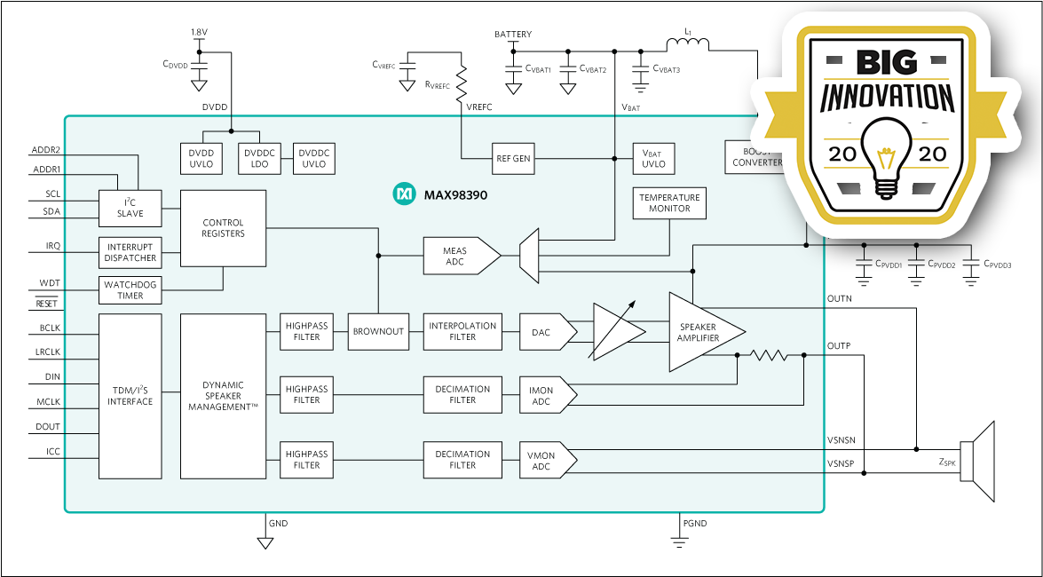

The MAX98390 is a high-efficiency mono Class-D DSM smart amplifier that features an integrated boost converter, integrated Dynamic Speaker Management™, and FET scaling for higher-efficiency at low output power.
The maximum boost converter output voltage is programmable from 6.5V to 10V in 0.125V increments from a battery voltage as low as 2.65V. The boost converter supports bypass mode for lower quiescent current and improved mid-power efficiency as well as envelope tracking which automatically adjusts the output voltage for maximum efficiency. The boosted supply efficiently delivers up to 6.2W at 10% THD+N into a 4Ω load.
Integrated IV sense and Dynamic Speaker Management allows louder, fuller audio while protecting the speaker against damage and improving sound quality.
The PCM interface supports I2S, left-justified, and 16-channel TDM formats as a slave or master device with I2C control. Either BCLK or MCLK can be used as the internal clock source providing system level flexibility.
Thermal and other status data can also be read from the I2C interface.
Patented active emissions limiting edge rate and overshoot control circuitry minimizes EMI and eliminates the need for output filtering found in traditional Class-D devices.
A flexible brownout-detection engine (BDE) can be programmed to initiate various current limiting, signal limiting, and clip functions to prevent dips in battery voltage. Threshold, hysteresis, and attack-and-release rates are programmable.
The MAX98390C is available in a 0.4mm pitch, 36-bump wafer-level package. The MAX98390D is available in a 0.5mm pitch, 30-bump wafer-level package. They are specified over the extended -40°C to +85°C temperature range.
![]() Design Solution: Unleash the Full Potential of Your Micro Speakers ›
Design Solution: Unleash the Full Potential of Your Micro Speakers ›

Applications
- Smartphones
- Tablets
- Notebook Computers
- Single Li-ion Cell Devices
- IoT Devices
- Toys
Applications
Consumer Technology Solutions
- Personal Electronics Solutions
Healthcare Solutions
- Therapy Device Solutions for Healthcare
Intelligent Building Solutions
- Automatic Identification and Data Capture (AIDC) Solutions
Dynamic Speaker Management (DSM) Solutions
Human Machine Interface Products
AD8233

The AD8233 is an integrated signal conditioning block for electrocardiogram (ECG) and other biopotential measurement applications. It is designed to extract, amplify, and filter small biopotential signals in the presence of noisy conditions, such as those created by motion or remote electrode placement. This design allows an ultralow power analog-to-digital converter (ADC) or an embedded microcontroller to easily acquire the output signal.
The AD8233 implements a two-pole, high-pass filter for eliminating motion artifacts and the electrode half cell potential. This filter is tightly coupled with the instrumentation amplifier architecture to allow both large gain and high-pass filtering in a single stage, thereby saving space and cost.
An uncommitted operational amplifier enables the AD8233 to create a three-pole, low-pass filter to remove additional noise. The user can select the frequency cutoff of all filters to suit different types of applications.
To improve the common-mode rejection of the line frequencies in the system and other undesired interferences, the AD8233 includes a right leg drive (RLD) amplifier for driven electrode applications.
The AD8233 includes a fast restore function that reduces the duration of the otherwise long settling tails of the high-pass filters. After an abrupt signal change that rails the amplifier (such as a leads off condition), the AD8233 automatically adjusts to a higher filter cutoff. This feature allows the AD8233 to recover quickly, and therefore, to take valid measurements soon after connecting the electrodes to the subject.
The AD8233 is available in a 2 mm × 1.7 mm, 20-ball WLCSP package and a 150 μm thin die for height constrained applications. Performance is specified from 0°C to 70°C and is operational from −40°C to +85°C.
APPLICATIONS
- Fitness and activity heart rate monitors
- Portable ECG
- Wearable and remote health monitors
- Gaming peripherals
- Biopotential signal acquisition, such as EMG or EEG
Applications
Healthcare Solutions
- Activity Tracking and Fall Detection Solutions
- Respiration Rate Measurement Solutions
- Therapy Device Solutions for Healthcare
- Vital Signs Monitoring Solutions
- Electrocardiogram (ECG) Measurement Solutions
- Non-Invasive Blood Pressure (NIBP) Solutions
- Wearable Health Monitor Solutions
Industrial Automation
- Programmable Logic Controllers (PLC) and Distributed Control Systems (DCS)
- Field Instrument Systems
Consumer Technology Solutions
- Extended Reality (XR) Solution for Edge Devices
Precision Technology Solutions
- Compact Low Power Precision Solutions
ADAU1860/ADAU1860-1
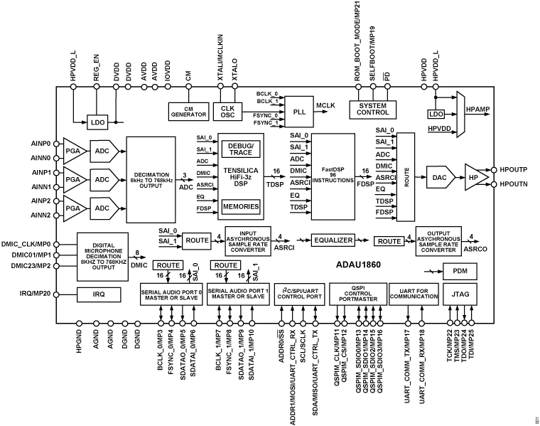
The ADAU1860/ADAU1860-1 are codecs with three inputs and one output that incorporate two digital signal processors (DSPs). The path from the analog input to the DSP core to the analog output is optimized for low latency and is ideal for noise canceling earphones. With the addition of just a few passive components, the ADAU1860/ADAU1860-1 provide a complete earphone solution.
APPLICATIONS
- Noise canceling handsets, headsets, and headphones
- Bluetooth active noise canceling (ANC) handsets, headsets, and headphones
- Personal navigation devices
- Digital still and video cameras
- Musical instrument effect processors
- Multimedia speaker systems
- Smartphones
Applications
Consumer Technology Solutions
- Smart Home Solutions
- Home Theater and Gaming Solutions
- Hearable and Wearable Solutions
Aerospace and Defense Systems
- Military Communication Solutions
ADIS16500
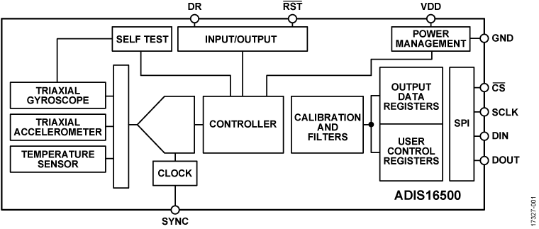
The ADIS16500 is a precision, miniature microelectromechanical system (MEMS) inertial measurement unit (IMU) that includes a triaxial gyroscope and a triaxial accelerometer. Each inertial sensor in the ADIS16500 combines with signal conditioning that optimizes dynamic performance. The factory calibration characterizes each sensor for sensitivity, bias, alignment, linear acceleration (gyroscope bias), and point of percussion (accelerometer location). As a result, each sensor has dynamic compensation formulas that provide accurate sensor measurements over a broad set of conditions.
The ADIS16500 provides a simplified, cost effective method for integrating accurate, multi-axis inertial sensing into industrial systems, especially when compared with the complexity and investment associated with discrete designs. All necessary motion testing and calibration are part of the production process at the factory, greatly reducing system integration time. Tight orthogonal alignment simplifies inertial frame alignment in navigation systems. The serial peripheral interface (SPI) and register structure provide a simple interface for data collection and configuration control.
The ADIS16500 is available in a 100-ball, ball grid array (BGA) package that is approximately 15 mm × 15 mm × 5 mm.
Applications
- Navigation, stabilization, and instrumentation
- Unmanned and autonomous vehicles
- Smart agriculture and construction machinery
- Factory/industrial automation, robotics
- Virtual/augmented reality
- Internet of Moving Things
Applications
Aerospace and Defense Systems
- Avionic Systems
- Missiles and Precision Munitions
- Phased Array Technology
- Aerospace and Defense Radar Systems
- Unmanned Aerial Vehicles (UAV)
Healthcare Solutions
- Medical Imaging Solutions
- Ultrasound Solutions
Industrial Automation
Consumer Technology Solutions
- Extended Reality (XR) Solution for Edge Devices
ADI Support
Let us know what you need help with, and we will share the best answers from the ADI knowledge database.
Get Help
{{modalTitle}}
{{modalDescription}}
{{dropdownTitle}}
- {{defaultSelectedText}} {{#each projectNames}}
- {{name}} {{/each}} {{#if newProjectText}}
-
 {{newProjectText}}
{{/if}}
{{newProjectText}}
{{/if}}
{{toggleButtonDescription}}
{{newProjectTitle}}
{{projectNameErrorText}}