Why Realistic Voltage Sources Should Be Considered When Designing a Reliable Power Supply
Why Realistic Voltage Sources Should Be Considered When Designing a Reliable Power Supply
Jun 1 2021
A power supply’s source, in actual use, is never ideal. The real behavior, including parasitics, needs to be considered to build a reliable power system. When we use power supplies, we ensure that a DC-to-DC converter, such as a switching regulator, can withstand a certain input voltage range and that it can generate the required output voltage from it with sufficient current. The input voltage is frequently specified as a range because it is usually not regulated exactly. For a power supply to function reliably, however, there must always be an input voltage within the permissible range available to the switching regulator.
For example, a typical input voltage range for a 12 V supply voltage may lie between 8 V and 16 V. Figure 1 shows a step-down converter (buck topology) that generates 3.3 V from a nominal voltage of 12 V.

Figure 1. A step-down switching regulator shown together with the (DC) voltage source of the system.
However, when designing the DC-to-DC converter, it is not sufficient to only consider the input voltage minimum and maximum values. Figure 1 shows that the buck converter has a switch at its positive input. This switch is turned on or off. The switching speed should be as high as possible so that only low switching losses occur. However, this causes a pulsed current to flow on the supply line. Not every voltage source can deliver these pulsed currents without any problems. As a result, voltage drops occur at the input of the switching regulator. To minimize this, backup capacitors are required right at the input of the power supply. Such a capacitor is shown as CIN in Figure 1.
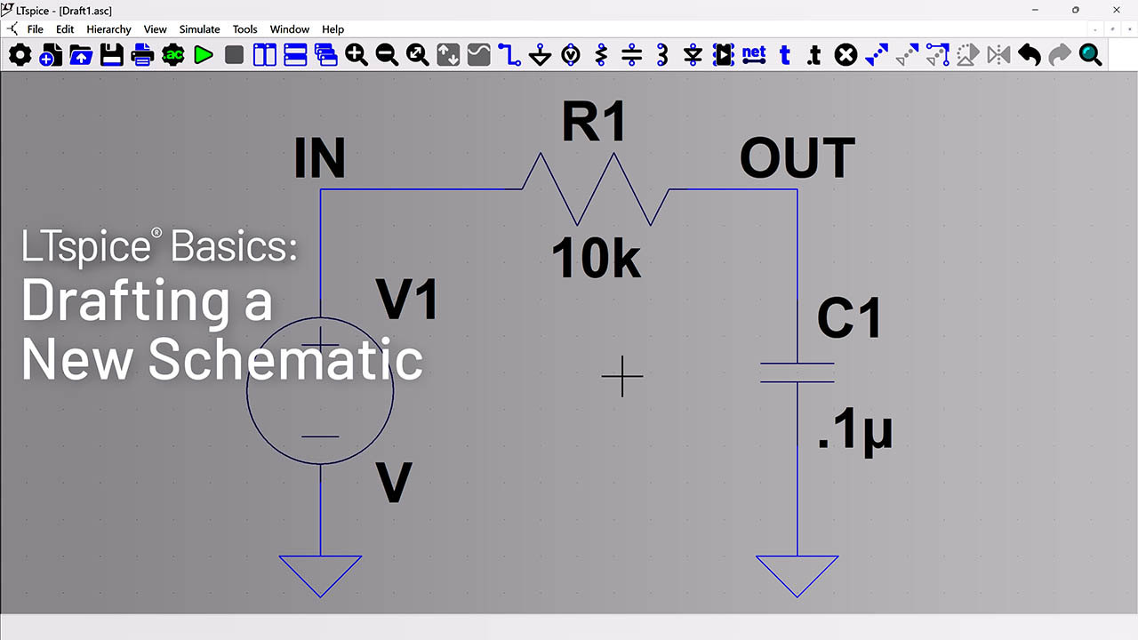
Figure 2 shows the circuit from Figure 1, but this time with the parasitic elements of the supply line and the voltage source itself. Both the internal resistance of the voltage source (RSERIES), the inductance and the resistance of the supply line (R, L supply line), and any current limitation are key characteristics of the voltage source that must be taken into account to guarantee trouble-free operation of the switching regulator. For the most part, the correct selection of the input capacitors can ensure proper operation of the circuit. The first approach should be to take the recommended capacitance value for CIN from the data sheet for a switching regulator IC. However, if the voltage source or the supply line exhibits special characteristics, it makes sense to simulate the combination of the voltage source and the switching regulator. Figure 3 shows a simulation performed with the LTspice® simulation environment from Analog Devices.

Figure 2. The circuit from Figure 1, but with the parasitic elements of the supply line and the voltage source shown.

Figure 3. A simulation with LTspice for checking the behavior of the input voltage of a switching regulator.
A simulation circuit for the ADP2360 buck converter is shown in Figure 3. The simplified form, in which the input voltage IN is generated with an ideal voltage source, is shown here. Because no internal resistance is defined for the voltage source and no parasitic values are given for the supply line between the voltage source and the switching regulator, the defined voltage is always applied to the VIN pin of the ADP2360. Therefore, it is not necessary to add an input capacitor (CIN). However, in the real world, an input capacitor is always required with a switching regulator because the voltage source and the supply line are not ideal. If a simulation environment such as LTspice is also used for checking the behavior with different input capacitors, a voltage source with internal resistance and a supply line with parasitic values for resistance and inductance, as shown in Figure 2, must be used.
About The Authors
Frederik Dostal is a power management expert with more than 20 years of experience in this industry. After his studies of microelectronics at the University of Erlangen, Germany, he joined National Semiconductor in 2001, w...
Related to this Article
Resources
{{modalTitle}}
{{modalDescription}}
{{dropdownTitle}}
- {{defaultSelectedText}} {{#each projectNames}}
- {{name}} {{/each}} {{#if newProjectText}}
-
{{newProjectText}}
{{/if}}
{{newProjectTitle}}
{{projectNameErrorText}}

