Understanding Power Monitor Accuracy
Measurement of a system’s power consumption during a final factory test (before deployment into the field) is a prudent part of a test program for any product. But there is an increasing emphasis to bring this functionality into the product itself for “run-time” monitoring of power, current, supply voltage, and energy. Accurate monitoring of these parameters provides valuable diagnostic information for scheduling maintenance and predicting failures. It can also assist in ensuring “green” systems are meeting their low power consumption goals. Analog Devices offers a range of products that provide run-time measurements of voltage, current, power and energy. These include stand-alone monitors such as the LTC2945, LTC2946 and LTC4151, or products that combine these features with hot swap functionality such as the LTC4215 (for +12V systems), the LTC4260 (for +48V systems) and the LTC4261 (for –48V systems). All of these devices essentially function as “multimeters on a chip”, but how accurate are they?
The Accuracy Specification Dilemma
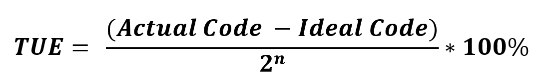
All of these products specify the Total Unadjusted Error (TUE) of their measurement channels, where TUE is the worst-case error, measured across all process parameters and temperatures and including errors from all sources combined into a single specification. It is usually described as a percentage of full-scale.
TUE simplifies preliminary error analysis by providing a maximum bound on the worst-case error across all conditions expressed in a single number.
However, since TUE is a single specification it often leads to confusion about measurement accuracy across the entire input range. Often a false assumption is made that the TUE error will occur throughout the input range of the converter resulting in gross inaccuracy at the lower end of the input range. Taking the LTC2946 energy monitor as an example, the TUE specification of the ΔSENSE channel is specified at 0.6% of full-scale. While this value might be fine for inputs near full-scale, it may not be acceptable for small inputs. TUE is only part of the story – other guaranteed specifications will constrain the allowable error to a smaller value when the input is less than full-scale.
To shed light on performance across the input range, an understanding of the various ADC error sources is necessary. This article will consider the LTC2946 configured for a 10.24A current measurement as an example, and will focus on the DC error specifications that are most relevant to power monitoring applications. The current sense channel is the most involved measurement to study because it includes errors internal to the LTC2946 as well as the tolerance of the sense resistor, and supply current is a parameter that is likely to vary widely during the operation of a system.
Error Sources And Specifications
Figure 1 shows the specification table in the LTC2946 datasheet. The specifications relevant to our analysis are TUE, Full-Scale Voltage, LSB Step Size, Offset Error, and INL.

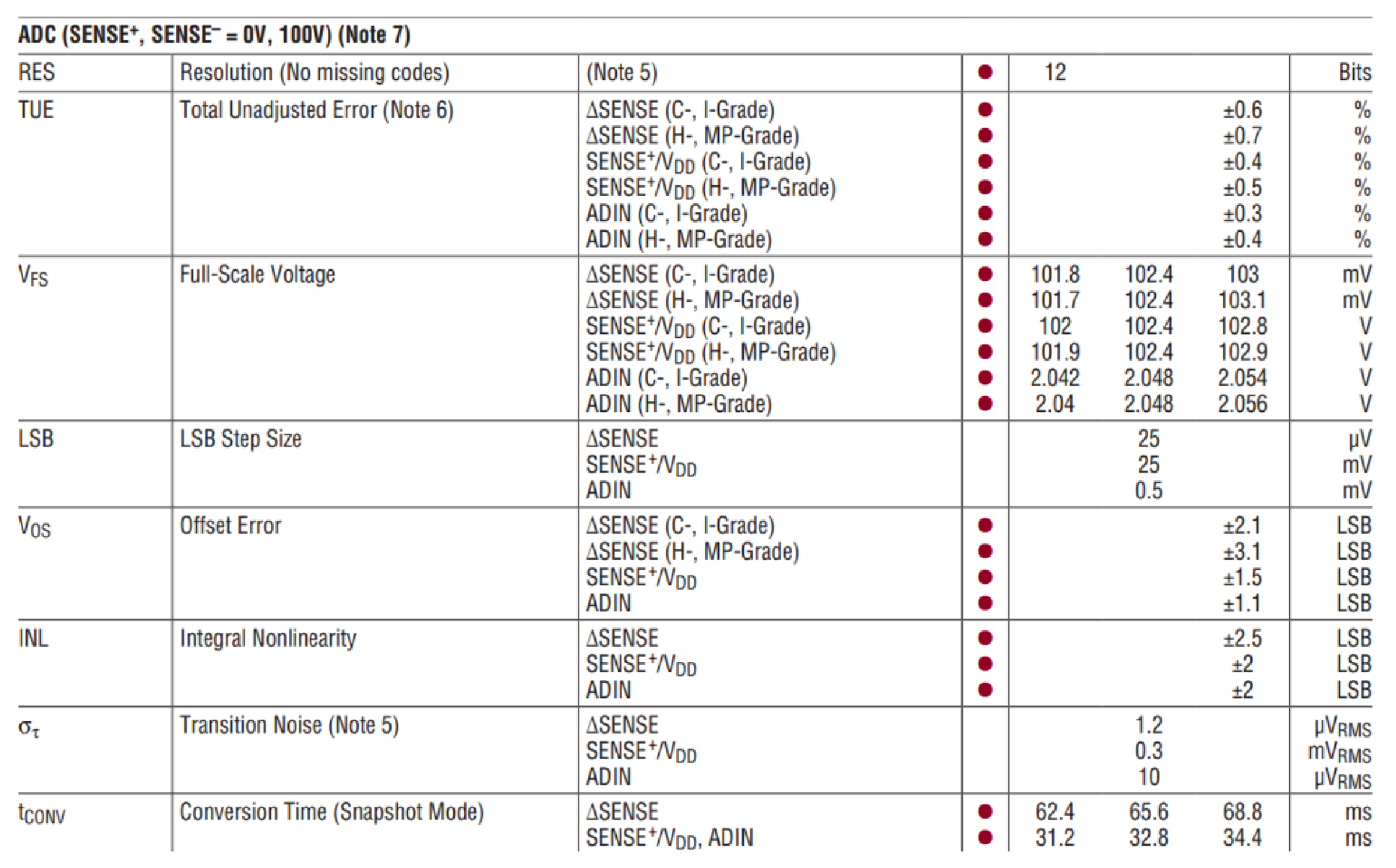
Figure 1. LTC2946 Specification Table
These specifications include contributions from all errors internal to the LTC2946, including the ADC, reference, current sense op amp (for the ΔSENSE channel), and internal dividers (for the SENSE+/VDD channel). Figure 2 shows the block diagram of the LTC2946, as well as an external 10mΩ, 1% tolerance sense resistor.

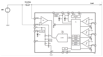
Figure 2. LTC2946 Block Diagram Showing Signal Chain
A useful concept for this analysis is the idea of a transfer function. This is the mapping of the input voltage between the SENSE+ and SENSE– pins to the digital output code. Figure 3 shows a hypothetical perfect transfer function, where a zero input produces an output code of zero counts, a full-scale input of 102.4mV produces an output code of 4095 counts, and there is a perfectly linear relationship between these points. Each code transition occurs exactly 25µV above the previous transition. In this perfect LTC2496, there is never an error greater than 1LSB1. The errors described next are all departures from this ideal.
1 The ideal transition from code 0 to code 1 occurs at 25µV for the LTC2946. Some ADCs are trimmed to give an ideal transition at ½ LSB input.

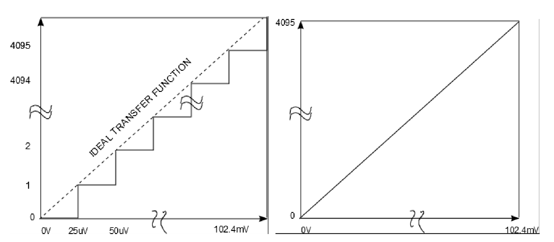
Figure 3. Zoomed In Transfer Function; Figure 3b: Entire Transfer Function
Offset Error Determines The Ability To Accurately Measure Small Currents
Offset is the output code of the LTC2946 that results when the input is zero. In the case of the LTC2946 this error has a maximum value of 2.1LSB, or 52.5uV. This equates to 0.057% error – about 10% of the TUE spec.


Figure 4. Positive and Negative Offset Error
Note that the offset may be positive or negative. If the offset is positive, the output code will be nonzero when the input is zero. If the offset is negative, the ADC will be “clamped” or “railed” at zero, and it will take some small voltage at the input to produce a nonzero output. For this reason, the offset must be evaluated with a small, known voltage applied to the input. This voltage is subtracted from the ADC reading to calculate the offset. Consider an LTC2946 with a worst-case negative offset; applying a voltage equal to 10 LSBs (250µV) would result in an output code 7.9 LSBs. Subtracting 10 LSBs from this output code results in –2.1 LSB. Similarly for a LTC2946 with a positive offset, the output code would be 12.1 LSBs, subtracting 10 LSB’s would result in the +2.1LSB offset.
It is true that applying this voltage allows other error sources to contaminate the measurement (Gain Error, Linearity) but the test voltage is chosen such that the offset error is still dominant and the additional errors are negligible.
The effect of offset on our 10.24A application is that when zero current is flowing through the sense resistor, an LTC2946 with a positive offset may indicate a current as high as 5.25mA, and an LTC2946 with a negative offset may continue to read zero until 7.75mA is flowing. The sense resistor’s tolerance does not affect the current measurement when the current is zero, and has minimal effect for small currents. That is, the LTC2946 offset is the dominant error source for small currents.
Full-Scale Error Determines The Ability To Accurately Measure Large Currents
Full-Scale Error is the error in the LTC2946 output code that results when an ideal full-scale voltage of 102.4mV is applied across the SENSE inputs. Full-Scale Error includes all error sources internal to the LTC2946: Offset (described previously), Gain Error, and INL(to be defined shortly.) The Full-Scale Error of the sense input is specified in terms of the input voltage that will result in a full-scale output: a part with negative Full-Scale Error will output a code of 4095 when the input is 103mV, and a part with a positive Full-Scale Error will output a code of 4095 when the input is 101.8mV. This specification can be “inverted” to be expressed in terms of the code that will result from a perfect 102.4mV input. An input of 102.4mV may produce an output code indicating a value from a minimum of 101.8mV (output code of 4071) and a maximum of 103mV (output code of 4119).
Note that in the maximum case, the output code will be “clamped” at 4095, in the same way that the output of a part with negative offset will be clamped at zero. In this regard Full-Scale Error is similar to offset error i.e. Full-Scale Error is the endpoint error at full-scale input whereas the Offset Error is the endpoint error at zero input. The Full-Scale Error spec for the LTC2946 is ±0.58% - slightly less than the 0.6% TUE spec.
Why isn’t the TUE spec simply 0.58%? The additional 0.02% error allowed by the TUE spec allows for the nonlinearity of the transfer function, which will be discussed shortly.
One additional error source must be considered to calculate the effect of Full-Scale Error on our 10.24A application – the sense resistor’s tolerance. A current of exactly 10.24A flowing through a 1% tolerance, 10mΩ resistor will produce a voltage as low as 10.24*0.01*0.99 = 92.16mV or as high as 10.24*0.01*1.01 = 103.42mV. The error in this voltage will add directly to the LTC2946’s Full-Scale Error, which will then be reflected in the output code. Thus the measured current can be as low as 10.24 * 0.99 * (0.9942) = 10.079A or as high as 10.24*1.01*1.0058 = 10.402A. Of course the high case will be clamped at an indicated current of 10.24A, so we can calculate the actual current that would produce the full-scale output code: 101.8mV / (0.01 * 1.01) = 10.079A; any current higher than this will continue to output a code of 4095.

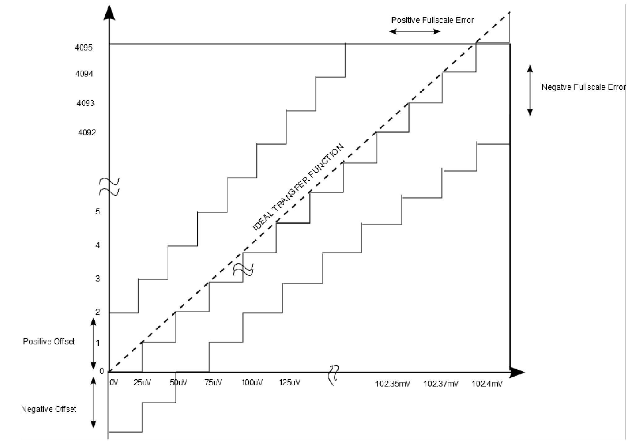
Figure 5. Full Scale Error.
Gain Error Is Often Less Useful Than Full-Scale Error
Gain Error is the difference in slope between the ideal transfer function and the actual transfer function as shown in Figure 6a. It requires two points along the transfer function to calculate, preferably close to the endpoints to account for the whole input range. Gain Error, as a datasheet specification, is often not as useful as Full-Scale Error for DC current and voltage measurements as it is possible to have zero Gain Error when the Offset and Full-Scale Errors are equal. This is illustrated in Figure 6b, which shows the transfer function of a device that has an Offset Error, a Full Scale Error, but perfect gain.
The LTC2946 current measurement application has four sources of Gain Error. Three are internal to the LTC2946: the reference, the sense amplifier’s gain of 20, and the ADC itself. The tolerance of the external sense resistor also directly affects the gain of the current measurement.


Figure 6a. Non-Zero Gain Error

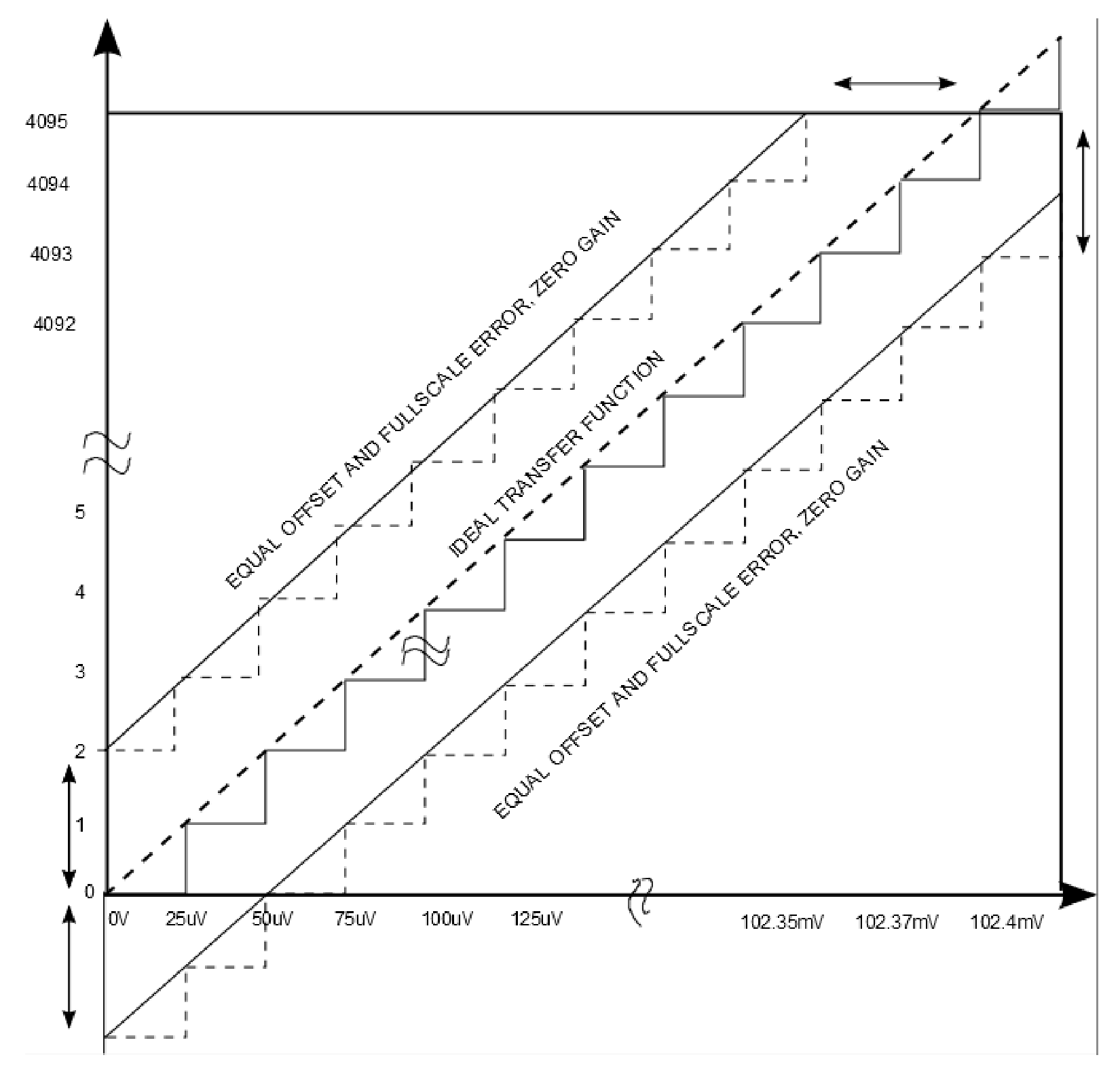
Figure 6b. Zero Gain Error
The Gain Error is not specified separately in the LTC2946 datasheet. However it can be estimated using the following equation:
Gain Error = Full-Scale Error – Offset Error
Noting the magnitude of the Offset and Full-Scale Errors, Gain Error is the dominant term in the Full-Scale Error spec.
Integral Nonlinearity Is The Deviation Of The Transfer Function From A Straight Line
Integral Nonlinearity (INL) is defined as the deviation of a code transition from its ideal transition point, without considering Offset Error and Full-Scale Error, as shown in Figure 7.

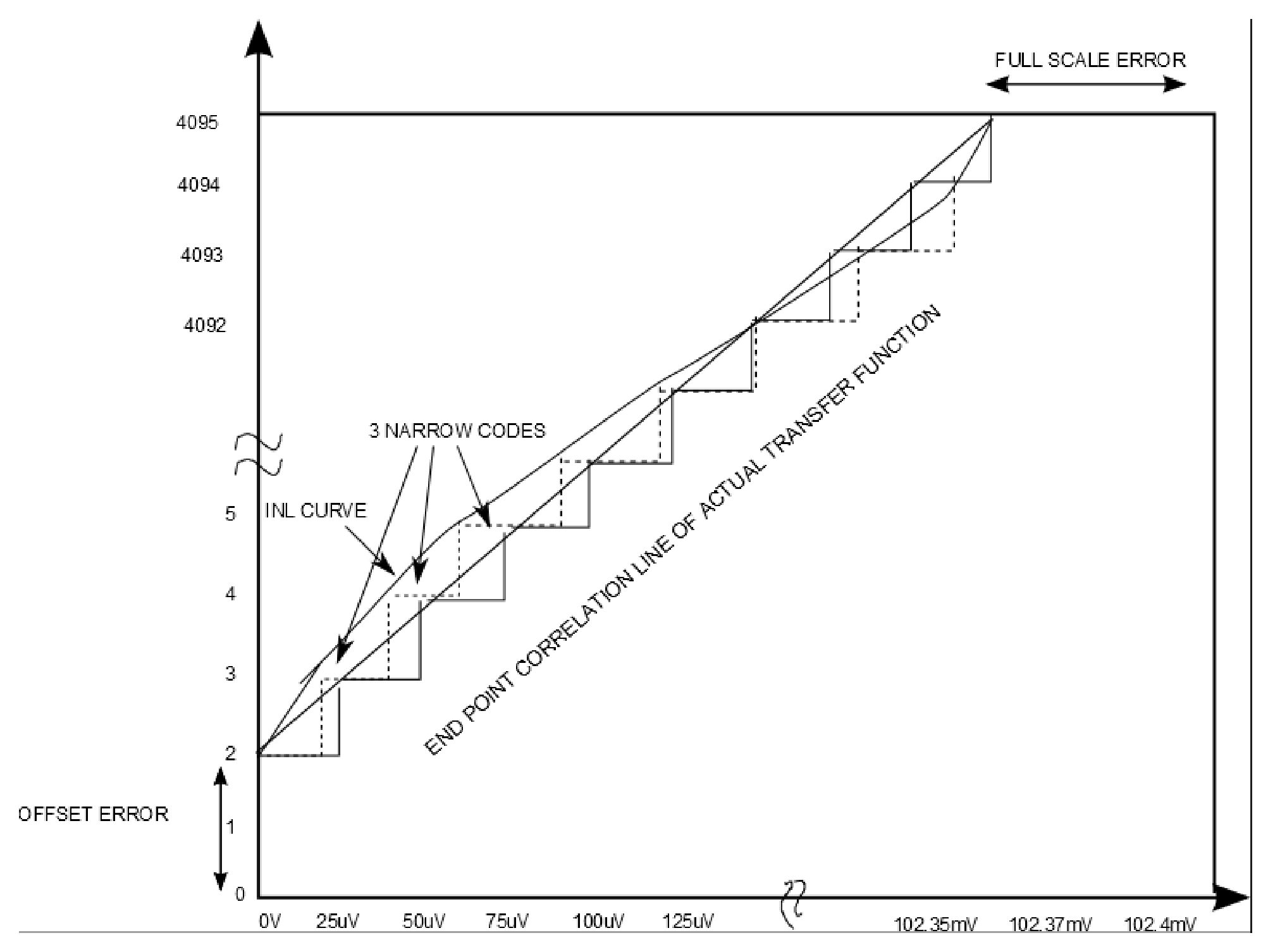
Figure 7. INL Error
The “shape” of the INL curve is determined by the architecture of the ADC. The LTC2946 has a first-order delta-sigma ADC, which tends to produce INL curves that are qualitatively similar from device to device. The typical INL curve shown in Figure 8 has a single “bow”, with INL error building gradually to a maximum near the center of the transfer function. Thus while the datasheet specification would allow a part to have a maximum INL error just a few codes away from either endpoint, actual devices will not behave in this way.

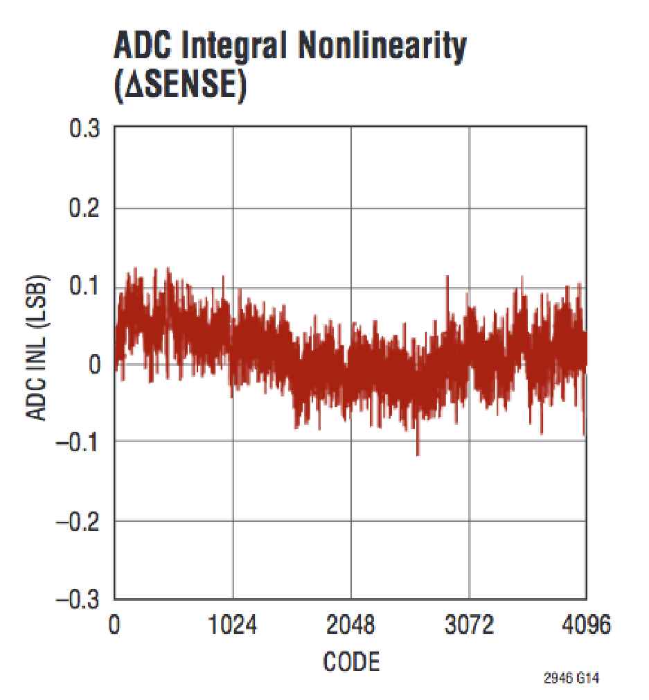
Figure 8. Typical LTC2946 INL
The impact of the LTC2946’s 2.5LSB INL specification on a typical current monitoring application is minimal. 2.5LSBs is equivalent to 6.25mA in our 10.24A example application, which is on par with the Offset Error, and insignificant compared to the 161mA Full-Scale Error.
Putting It All Together
Consider our 10.24A LTC2946 example on a telecom board that draws 5A when no data is being processed, and 9A under full load. The LTC2946 with a 10mΩ resistor for 10.24A full-scale is a good fit, leaving some room for higher current transients. If TUE was the only error specified, the measurement error could be as much as 164mA, for any input current (including the error contributed by the sense resistor.) An error of 164mA in a 9A current measurement is fairly good, about 1.8% of the actual current, and the error would be dominated by the 1% tolerance of the sense resistor. At 5A, the 164mA error would represent 3.22% of the actual current, still adequate for a “state of health” measurement. However, if the application has a very low power sleep state or other operating modes that draw significantly less current, then a 164mA error is bothersome.
Applying the other specifications defined previously shows that the measurement error is considerably better than the TUE spec at low currents. With zero current flow, there is zero voltage across the sense resistor and the maximum error will be determined by the offset specification of 2.1LSB. Multiplying this number by the 25µV LSB gives an offset of 52.5µV which results in a maximum error of 5.2mA assuming a perfect sense resistor of 10mΩ.
Similarly, the maximum error seen at full-scale would be bounded by the Full-Scale Error and result in an error of 161mA as calculated previously.
The remaining error is caused by the INL which results in the departure of the transfer function from the ideal straight line between its end points. The LTC2946’s INL spec for the ΔSENSE channel is 2.5LSB, or 62.5µV. This translates to an error of 5.2mA for a 10mΩ sense resistor. Note that the INL error will be at a maximum somewhere along the transfer function (see Figure 8) but its contribution will be small for inputs close to zero or full-scale.
This means, for a 10A application if we were to introduce the error introduced by a 1% resistor we would measure low currents with an accuracy of about 6.3mA. The dominant error for small inputs being the Offset Error, and for larger inputs the Full-Scale Error of the LTC2946 and the tolerance of the sense resistor.
Figure 9 was generated by a handy error calculator spreadsheet accompanying this document. It calculates the maximum error that can be expected for any voltage within the device’s input range. The inputs to the spreadsheet are TUE, Full-Scale Error, Offset Error, and INL. One additional parameter called the “INL Build Rate” is required to estimate the contribution of INL. This parameter, expressed as a percentage of the transfer function, allows the INL error to build from zero contribution at the zero-scale and full-scale to a maximum close to the center of the transfer function. Entering a value of zero will produce a more conservative result; entering a value of 30 will more closely model actual LTC2946s.


Figure 9. Actual Error vs.TUE
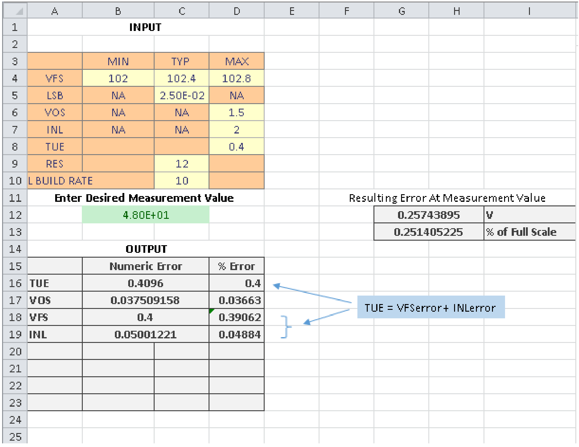
Voltage Measurement Accuracy
The same analysis applies to voltage measurements as well. The 0.4% TUE spec for the SENSE+/VDD channel sounds like a good number for a power supply output; 1% is considered very accurate for a low voltage linear regulator, and a 0.4% accurate measurement of a 48V telecom supply is more than adequate, considering most loads will accept 36V to 72V. But 48V is about in the middle of the LTC2946’s VIN measurement range of 102.4V; if the 0.4% TUE was the only specification, the relative impact to the measurement would be approximately double:
48V measurement error = 0.4% * (102.4 / 48V) = 0.8%
This is still good for a 48V supply, but entering the LTC2946 specifications for the SENSE+ / VDD channel and a measurement input of 48V into the spreadsheet shows that the error is approximately 0.25% of full-scale.

Conclusion
Total Unadjusted Error is a convenient accuracy specification expressed as a single number. But an understanding of all accuracy specifications is essential for understanding what measurement errors to expect across the entire input range.
About the Authors
Related to this Article
Products
High Precision, Wide Bandwidth Current Measurement Signal Chain
Positive High Voltage Hot Swap Controller with I2C Compatible Monitoring
Negative Voltage Hot Swap Controllers with ADC and I²C Monitoring
Hot Swap Controller with I2C Compatible Monitoring
Hot Swap Controller with I2C Compatible Monitoring
High Voltage I2C Current and Voltage Monitor
Wide Range I2C Power, Charge and Energy Monitor
Wide Range I2C Power Monitor
Latest Media 21


