Abstract
In power electronics, thermal considerations are fundamental in the design of circuits and printed circuit boards. Yet, thermal aspects are often overlooked in signal-path electronics, even though they are just as important to device performance. This application note defines and discusses basic thermal properties. It also describes the thermal design issues that should be considered when using the MAX11500–MAX11509 family of low-cost video filters.
General Thermal Aspects and Some Definitions
All semiconductor devices dissipate heat to some degree. There are three paths through which heat is dissipated: package top to air, package bottom to board, and package leads to board. The dominant path for heat dissipation in the MAX11500, MAX11501/MAX11502, MAX11504/MAX11505 video filters is through the leads to the board.
Thermal resistance is a value for the thermal transfer properties of a material. It is referred to using the Greek letter Θ (theta), the first letter of the Greek word for heat, Θερµος (thermos).
The thermal resistance from the junction to case is, therefore, known as ΘJC. The thermal resistance from case to ambient is known as ΘCA, and the thermal resistance from junction to ambient is known as ΘJA. Thermal models are analogous to electrical models (Figure 1), and capacitance plays a part in both. Temperature is analogous to voltage, and heat is analogous to current.
In the electrical world, if current flows through a resistance, a voltage differential will be generated. Similarly, if heat flows through a thermal resistance, a temperature differential will be generated. In addition, if there is a short transient heat flow, the thermal capacitances will shunt the heat and there will be only a small temperature rise. Objects need time to heat up.
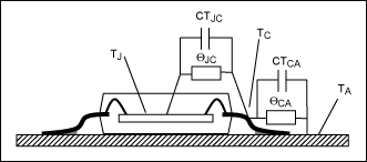
Figure 1. Electrical analogy of heat dissipation through device leads.
In most cases, ΘJC is smaller than ΘCA and CTJC is smaller than CTCA. This can be expressed mathematically as below. From now on we will ignore the capacitances and address steady-state situations, since these characteristics are more relevant to video filters.
ΘJA is generally used because packages are specified using a standard PCB defined in the relevant JEDEC standards, JES51-3 or JES51-7. (See more on the JEDEC standards in the Package Specification section below.)

Knowing the thermal resistance of a package allows us to calculate the junction temperature for a given power dissipation and ambient temperature. The problem in calculating junction temperature in ICs which rely on the PCB for heat dissipation, is knowing what the thermal resistance from junction to ambient actually is.
Consider a simple example. A device has VCC = 5.0V and draws 100mA. The maximum ambient temperature is 40°C and the maximum allowed junction temperature is 150°C. The power dissipation is expressed as:
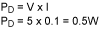
Assume that ΘJA = 150°C/W and that the equipment must operate at a very benign ambient temperature of

This temperature is well below the maximum die temperature, so the device will have no thermal problems. This process looks easy, but it is deceptively complex. With small ICs, we cannot be sure what the ΘJA actually is because it is dependant on the PCB layout.
Package Specifications
The text below shows the Absolute Maximum Ratings for the MAX11501 video filter driver, as shown in the product's data sheet.
Absolute Maximum Ratings
- VCC to GND......................................................-0.3V to +6V
All other pins to GND.....-0.3V to min of (VCC + 0.3V) and +6V
Continuous Power Dissipation (TA = +70°C)
8-pin SOIC (derate 5.9mW/°C above +70°C)............470mW
Maximum Current into any Pin except VCC and GND....±50mA - Operating Temperature Ranges:
MAX1150xUSA...............................................0°C to +85°C
Storage Temperature Range.........................-65°C to +150°C
Lead Temperature (soldering, 10s)..............................+300°C
Junction Temperature................................................+150°C
The key specifications for this discussion are Continuous Power Dissipation and Junction Temperature. The maximum junction temperature is 150°C and the maximum power that can be dissipated is 470mW at 70°C ambient. These conditions would result in a die temperature of 150°C.
Therefore, we can calculate ΘJA as:
This can be confirmed because ΘJA is simply the reciprocal of the derating factor.
All of this data comes from the JEDEC specification for the package. There are three specifications of interest for Analog video filters:
- EIA/JESD51-3, Low Effective Thermal Conductivity Test Board for Leaded Surface Mount Packages
- EIA/JESD51-5, Extension of Thermal Test Board Standards for Packages with Direct Thermal Attachment Mechanisms
- EIA/JESD51-7, High Effective Thermal Conductivity Test Board for Leaded Surface Mount Packages
Package specifications for the MAX11500–MAX11505 are shown in Table 1.
| Device | Single-Layer Board | Multilayer Board | ||||
| ΘJA/°C/W | ΘJC/°C/W | ΘCA/°C/W | ΘJA/°C/W | ΘJC/°C/W | ΘCA/°C/W | |
| MAX11500 | 170 | 40 | 130 | 136 | 38 | 98 |
| MAX11501 | 170 | 40 | 130 | 136 | 38 | 98 |
| MAX11502 | 170 | 40 | 130 | 136 | 38 | 98 |
| MAX11504 | 180 | 42 | 138 | 113 | 42 | 71 |
| MAX11505 | 180 | 42 | 138 | 113 | 42 | 71 |
The Problem with Video Signals and ICs in Practical Situations
The JEDEC specifications detail the standard PCB used to test a device. This specification allows devices to be compared and specified in a defined way. However in practice, it is highly unlikely that a device will be mounted on a board with the same thermal characteristics as the JEDEC-specified board. The board certainly will not have the same layout.
A typical layout is shown below. This PCB is used in the evaluation (EV) kit for the MAX11501 3-channel SD Filter Driver.
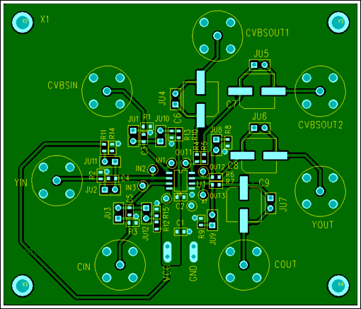
Figure 2. MAX11501 evaluation board.
Pins 4 and 5 are connected to a large area of copper with maximum area. These are the power and ground pins that dissipate most of the power. This device does not have a thermal pad on the underside.
Calculating Power Dissipation
Power dissipation in these video filters comes from two sources: quiescent and signal. Calculating the quiescent dissipation is easy. The data is available directly from the data sheet.
The data sheet for the MAX11501 states the supply current at VCC = 5.0V: 18mA typical and 24mA maximum. Therefore, the quiescent power dissipation is 120mW maximum.
The power dissipation caused by the signal is defined by the equation:
Where:
- Pdo = power dissipated in the channel
- Vorms = rms voltage at the output of the channel
- Rl = load resistance of the channel
- VCC = device supply voltage
To calculate the device's total power dissipation we simply sum the dissipation of each channel and the quiescent dissipation of the device.
The procedure seems quite simple so far. But the unknown term is the RMS output voltage, which is dependant on the video material.
Worst-Case Video Signals
There are several signals that must be considered: CVBS, Y/C, RGB, and YUV.
The worst-case scenario is RGB with a 100% white picture driving double loads on each channel. This is the signal that we will consider.
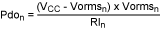
The line-based signal will look like Figure 3.
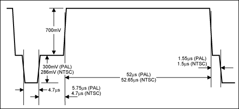
Figure 3. Video line waveform.
The PAL and NTSC vertical blanking intervals are represented in Figures 4 and 5, respectively.
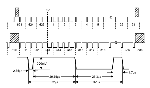
Figure 4. PAL vertical blanking and field synchronization pulses.
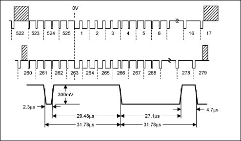
Figure 5. NTSC vertical blanking and field synchronization pulses. Note: NTSC is defined as having a minimum of 19H vertical blanking. It can, however, be longer.
Given the above information, we can calculate the RMS voltage of this signal. This will be done first for PAL.
The RMS voltage of a line is calculated below. This is normalized for a sync to a peak white level of 1V.

This value is valid for the 575 lines outside the vertical blanking period. We can calculate the RMS voltages of the lines inside the vertical blanking interval similarly. The results are shown below in Table 2, together with the final RMS calculation.
| Line Numbers | Number of Lines | RMS Voltage |
| 623 | 1 | 0.552 |
| 624, 625, 4, 5, 311, 312, 316, 317 | 8 | 0.278 |
| 1, 2, 314, 315 | 4 | 0.044 |
| 3 | 1 | 0.161 |
| 6-22, 318-335 | 34 | 0.278 |
| 23 | 1 | 0.562 |
| 313 | 1 | 0.161 |
| All Active Lines | 575 | 0.847 |
| Total | 625 | |
| Total RMS | 0.800 |
Table 3 shows a similar calculation for NTSC.
| Line Numbers | Number of Lines | RMS Voltage |
| 1, 2, 3, 264, 265 | 5 | 0.044 |
| 523, 524, 525, 4, 5, 6, 261, 262, 267, 268 | 10 | 0.278 |
| 7-16, 269-278 | 20 | 0.278 |
| 260 | 1 | 0.557 |
| 263 | 1 | 0.161 |
| 266 | 1 | 0.161 |
| All Active Lines | 487 | 0.858 |
| Total | 525 | |
| Total RMS | 0.814 |
If the sync tip is above 0V, we can simply add this offset to the final result to obtain the overall RMS value. Therefore, the total RMS voltage will be 80% for PAL and 81% for NTSC of the sync tip—peak white level plus any DC offset. Most practical engineers use 80% for all.
A Practical Example
Consider the worst-case example of a MAX11501 3-channel video filter used for a 625-line RGB signal.
The inputs and outputs are DC-coupled so that peak white at the input is 1.4V. This is the maximum allowed input voltage. We allow a 5% overhead so that the maximum sync tip to peak white at the input is 1.05V. Hence, we have the voltage levels as shown in Figure 6.
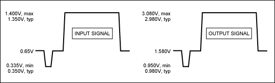
Figure 6. Example input and output voltages
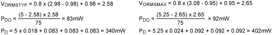
Now we can easily calculate the typical and maximum power dissipations:
- Calculate the RMS output voltages.
- Calculate the power dissipations per channel.
- Calculate the total power dissipation.
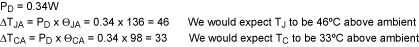
Now assuming that we have a good heatsink and are achieving close to the optimal heat dissipation, we can calculate the die temperature:

Clearly, the maximum of 137°C is unlikely to occur in practice. However we can now be satisfied that the die will not overheat even under worst-case conditions.
Practical Measurements
These measurements were done using the MAX11501 EV kit set up as below. Since this is a double-sided board, the thermal parameters for a multilayer board were used: ΘJA = 136, ΘJC = 38, ΘCA = 98. The board was mounted in still air.
Setup
- VCC = 5.0V
- Two video loads on each output
- Signal set to 525-line RGB, 100% white with sync on all channels
Theoretical Calculations
These calculations assume that the PCB thermal characteristics approximate those used to specify the package performance:
Results
- Quiescent Current ICC: 18mA
- Device Temperature measured at the ground pin: 63°C
- Ambient Temperature: 25°C
Calculations
We can now calculate the ΘJA value for the system. This value will tell us how close our board is to the ideal used in specifying the package:

We see that our PCB is performing slightly less efficiently than the ideal. We can now use the total ΘJA for our system to calculate die temperature at the maximum ambient, say 70°C.

Conclusions
We have shown that the RMS voltage of a worst-case video signal can be approximated to 80% of the sync-tip to peak white level, plus any offset.
We have also shown a method of measuring the thermal performance of our board and applied that to a design to ensure that the die temperature of our device stays within design limits.
{{modalTitle}}
{{modalDescription}}
{{dropdownTitle}}
- {{defaultSelectedText}} {{#each projectNames}}
- {{name}} {{/each}} {{#if newProjectText}}
-
 {{newProjectText}}
{{/if}}
{{newProjectText}}
{{/if}}
{{newProjectTitle}}
{{projectNameErrorText}}
Latest Media 20