Abstract
Application of the MAX2242 power amplifier (PA) is described in detail. Included topics are: PCB layout, interstage matching, thermal management, and the ultra chip-scale package. PA delivers +22dBm output power, with ACPR of < -33dBc on the first side lobe with CCK modulation. On-chip power detector gives a 20dB dynamic range. Operating supply voltage is between 2.7V and 3.6V. FR4 circuit board material is used. Thorough grounding is critical for high frequency, high power circuits. Sample layout is shown for best performance. Simulation of entire input network allows matching circuit design. Bypass capacitors are needed on the power supply lines for both low and high frequencies. UCSP™ drawing is shown with 0.5mm ball pitch. MAX2242 test set up uses spectrum analyzer to measure side lobe levels, and RF power meter to measure the power output.
Overview
The intent of this application note is to provide design engineers with application information for the MAX2242 power amplifier. A range of topics are covered, including printed-circuit-board layout, interstage matching, input and output impedance, thermal management, and the ultra-chip-scale package.
General Description
The MAX2242 is a linear power amplifier (PA) designed for 2.4GHz ISM-band wireless LAN applications. It delivers 22.5dBm of linear output power with an adjacent-channel power ratio (ACPR) of < -33dBc first-side lobe and < -55dBc second-side lobe, compliant with the IEEE® 802.11b 11MB/s WLAN standard. The PA is packaged in the 3 x 4 ultra-chip-scale package (UCSP), measuring only 1.5mm x 2.0mm, which is ideal for radios in small PC cards and compact flash card form factors.
The MAX2242 power amplifier consists of a three-stage PA, a power detector, and power-management circuitry. The power detector provides more than 20dB of dynamic range with ±0.8dB of accuracy at the highest output power level. An accurate automatic power level control (ALC) function can be implemented easily using this detector circuit.
The PA also features an external bias-control pin. Through the use of an external DAC, the current can be throttled back at lower output power levels while maintaining sufficient ACPR performance. As a result, the highest-possible efficiency is maintained at all power levels. The device operates over a single +2.7V to +3.6V power-supply range. An on-chip shutdown feature reduces operating current to 0.5µA, eliminating the need for an external supply switch.
Applications
- IEEE 802.11b
- Wireless LANs
- Home RF
- 2.4GHz cordless phones
- 2.4GHz ISM radios
Features
- Po = 22.0dBm linear output power (ACPR ≤ -33dBc first-side lobe and ≤ -55dBc second-side lobe)
- 28dB gain
- On-chip power detector
- External bias control for current throttleback
- +2.7V to +3.6V single-supply operation
- Ultra-small-chip-scale package (UCSP), 1.5mm x 2.0mm
Design Considerations
There are many factors that need to be considered when designing an RF power amplifier. The following design considerations and resources (discussed below) should be well understood before beginning the PC-board layout:
- PC-board material
- Grounding strategy
- Interstage matching
- Input and output impedance matching
- Transient stability
- Thermal management
- Ultra-Chip-scale package (UCSP)
- Amplifier test setup
- MAX2242 data sheet
- MAX2242 evaluation kit
PC-Board Material
The printed-circuit-board material should be either FR4 or G-10. This type of material is a good choice for most low-cost wireless applications for frequencies up to 3GHz. The MAX2242 evaluation board utilizes a four-layer FR4 with a dielectric constant of 4.5, a dielectric thickness of 6 mils, and 1oz copper.
Grounding Strategy
The necessity for good grounding cannot be emphasized enough. When designing RF power amplifiers, the technique used to ground the various components is so important that it requires special attention.
With low-impedance devices, you have to be more concerned with current flow, as opposed to high voltage in a high-impedance circuit. This means that ground current paths and the current handling capability of components have to be considered carefully. Remember, grounding becomes more critical at either high power levels or high frequencies. This application involves both conditions!
When designing with low-impedance circuits such as the MAX2242, which has an output impedance of approximately (8 + j5)Ω at 2.45GHz, it takes only about 0.5nH of inductance to equal 8Ω of inductive reactance. Eight ohm of reactance are produced by 60 mils x 10 mils of microstrip line on an FR4 PC board with a dielectric constant of 4.5 and a thickness of 6 mils.
Good grounding in this application means minimizing inductive reactance between the top component layer and the ground plane, forcing two different ground points to have a potential difference of 0V and preventing stray signals from coupling from one stage to the next.
Good grounding is achieved by ensuring that the ground plane is nearly continuous. The top-side ground should be connected to the bottom-side ground using multiple, plated through-hole vias. The MAX2242 has three ground pins: GND1, GND2, and GND3. All three should have ground through-hole vias located as near the device as possible to minimize the inductive reactance. The MAX2242 evaluation board utilizes 10 mil plated through-hole vias placed 4 mils from the edge of the ground through-hole vias to the edge of the three PA ground pins.
Figure 1 shows how multiple through-hole ground vias are used to improve the grounding of the board, minimizing the inductive reactance established between different board layers and also minimizing the inductive reactance of passive components by the through-hole ground vias being placed as close as possible to the components. In addition, it's very important to have ground vias along the RF path to enable movement of matching components in case optimizing is necessary.
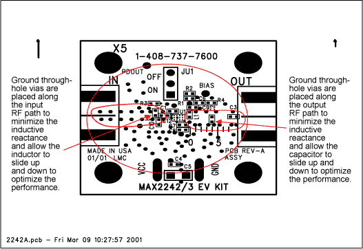
Figure 1. Top-component view of the MAX2242 evaluation board.
Interstage Matching
Off-chip interstage matching in multistage amplifiers is critical, because the intermediate stages are partially matched. A small amount of inductance in the form of a lumped or distributed element is required to optimize the predriver and driver amplifiers.
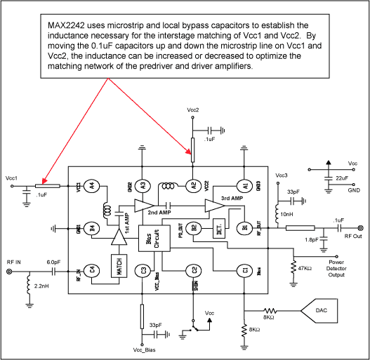
Figure 2. MAX2242 application circuit.
Input and Output Impedance Matching
The input and output impedance was achieved in two iterations. The first iteration was attained by small-signal simulation, and the second was reached through empirical tuning under large-signal conditions.
Figures 3 and 4 show the modeled lumped and distributed elements of the actual layout dimensions that make up the optimum input and output matching networks.
Figure 5 shows the simulated optimum source Z(1,1) and load Z(2,2) impedance from the actual layout. Z(1,1) and Z(2,2) should be used as the starting point for optimum source and load impedances.
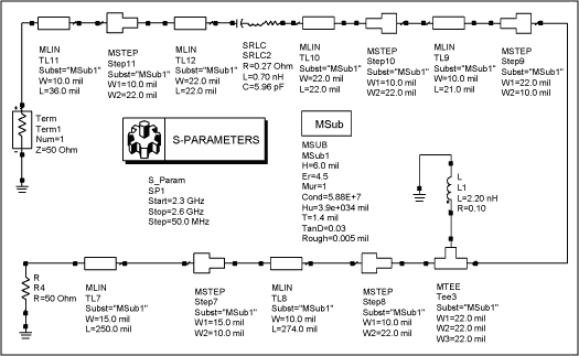
Figure 3. Input matching network.
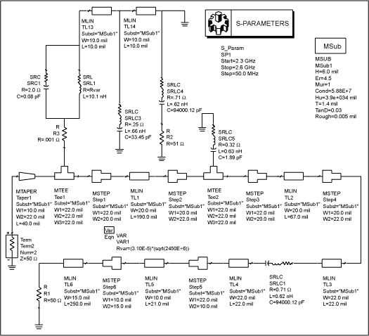
Figure 4. Output matching network.
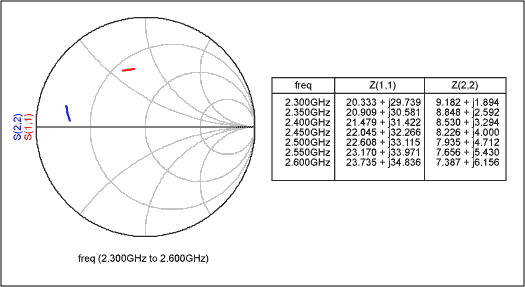
Figure 5. Optimum source and load impedance.
Transient Stability
Much attention has been given to improving transient stability. The following guidelines will prevent the MAX2242 from becoming unstable.
First of all, a large global bypass capacitor (tantalum or electrolytic), placed at the main VCC feed point to ground, prevents tendencies toward oscillations in the circuit. Also, it is very important to add local decoupling capacitors to the VCC feed points to ensure isolation from power-supply-related feedback.
Power-supply bias lines require proper shielding to prevent stray RF signals from coupling onto the bias lines. This is particularly important when 30dB or higher cascaded-gain stages are used in a multistage PA. Power-supply bias line shielding can be achieved by separating the VCC lines and, if possible, by routing the VCC lines on the bottom-side ground plane, where stray signals are minimal, or on one of the inner layers of the board, also where stray signals are minimal.
High-gain multistage amplifiers are susceptible to feedback where the output signal couples into the input path. At a frequency where phase shift totals 180 degrees, oscillations can occur. To minimize RF coupling from the output to the input, it is advisable to keep all RF lines as short as possible to lessen the antenna effect.
Finally, poor circuit board grounding can also be the cause of oscillations. Large PA currents flowing through non-zero ground impedance will induce a voltage, injecting noise into the ground system.
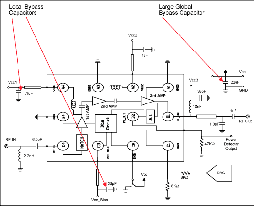
Figure 6. Application schematic with internal block diagram.
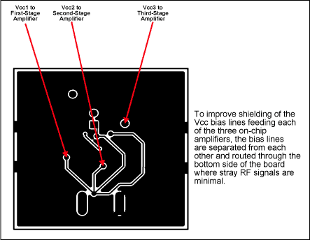
Figure 7. Bottom-side view of the MAX2242 evaluation board.
Thermal Management
Power transistors dissipate large amounts of power in their collector-base junctions. The dissipated power is in the form of heat, which raises the junction temperature. However, the junction temperature, TJ, must not be allowed to exceed a specified maximum, TJMAX; otherwise, the transistor could suffer permanent damage. Even if catastrophic failure does not occur, long-term reliability will be impacted. For silicon devices, TJMAX is about 150°C. The MAX2242, being a silicon-based device, uses 150°C as its maximum junction temperature, or TJMAX.
The MAX2242 utilizes its own evaluation-board ground plane as the heatsink.
Figure 8 can be seen as an analogy showing the electrical equivalent circuit of the thermal-conduction process. Power dissipation corresponds to current, temperature difference corresponds to voltage difference, and thermal resistance corresponds to electrical resistance.
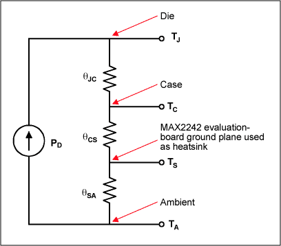
Figure 8. Electrical equivalent circuit of the thermal-conduction process.
TJ = (θJC + θCS + θSA) × PD + TA
Ultra-Chip-Scale Package (UCSP)
The MAX2242 is packaged in an ultra-chip-scale package. The principal advantage of this packaging technology is that the IC-to-PC-board inductance is minimized. The secondary benefits are the reduction in package size and manufacturing cycle time, as well as enhanced thermal-conduction characteristics.
For more information on UCSPs, please refer to the application note 1891, "Wafer-level packaging (WLP) and its applications."
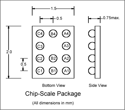
Figure 9. Ultra-chip-scale package.
Amplifier Test Setup
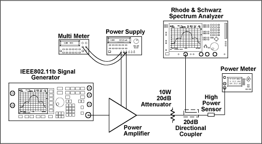
Figure 10. MAX2242 test setup.
Related to this Article
Products
Product Categories
{{modalTitle}}
{{modalDescription}}
{{dropdownTitle}}
- {{defaultSelectedText}} {{#each projectNames}}
- {{name}} {{/each}} {{#if newProjectText}}
-
 {{newProjectText}}
{{/if}}
{{newProjectText}}
{{/if}}
{{newProjectTitle}}
{{projectNameErrorText}}
Latest Media 21


