Abstract
Modern communications systems with multiport T1/E1/J1 line cards employ redundancy to achieve the high-availability telecom networks require. Traditionally, these systems have used relays to implement
Related application note: Intel(R) T1/E1/J1, N+1 Redundancy With Analog Switches and Intel(R) LXT38x Line Interface Units
| Relay | Analog Switch | |
| Board Space | 100mm2 | 15mm2 |
| Power Consumption | 140mW | 5µW |
| Switching Speed | 4ms | 30ns |
| Reliability | Mechanical Operation | No Moving Parts |
This application note shows how to implement T1/E1/J1, N+1 redundancy protection using analog switches. It provides guidelines for selecting analog switches for your application and shows test results using Analog switches and T1/E1/J1 transceivers.
Redundancy Architectures
Figures 1 and 2 show two redundancy architectures with analog switches. For clarity, there are separate drawings for the transmit and receive interfaces. Receive and transmit interfaces will reside in the same board for each T1/E1 port. The drawings represent the typical interface transformers and resistors recommended for a Analog transceiver such as the DS2155. In both cases, there is a protection bus running in the backplane where the input or output signals can be routed through the analog switches. The protection bus connects directly to a backup (protection) line card.
In Figure 1 ("Architecture A"), analog switches reside in the line cards themselves. Architecture A has the advantage of not requiring a separate line card for protection switching as in the "Architecture B" below. It does require that the switches be powered even through fail-over switching which could require a separate, dedicated power supply.

Figure 1a. Redundancy Architecture A: receive path.
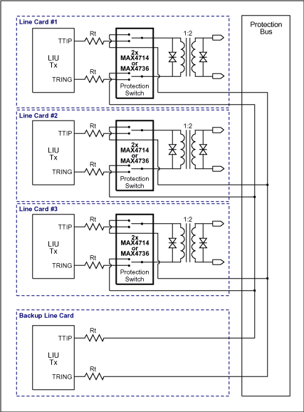
Figure 1b. Redundancy Architecture A: transmit path.
In Figure 2 ("Architecture B"), analog switches reside in a separate "Protection Switching Card". Architecture B has the advantage that it does not rely on the power being always "on" in the line cards themselves but it does require an extra protection switching card.

Figure 2a. Redundancy Architecture B: receive path.
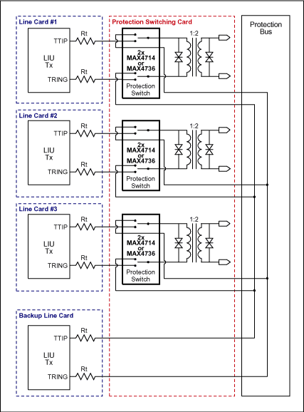
Figure 2b. Redundancy Architecture B: transmit path.
Analog Switch Selection
In order to meet the T1/E1/J1 interface specifications, the analog switches must be carefully selected for their electrical characteristics. Since the requirements for transmit and receive interfaces are quite different, we will examine them separately.
Transmit Interface Switch
In the transmit interface, the switch on resistance (RON) is a critical parameter. In Figures 1 and 2 we can see that the switch RON is in series with the output driver and the transformer primary and therefore, can cause a slight reduction in the output pulse amplitude. In most cases, the amplitude reduction can be compensated by simply reducing the series resistors (RT) by an amount corresponding to the switch typical RON value. As an example, if the transceiver recommended RT is 11Ω and RON (typ) is 0.5Ω then the actual RT value should be 10.5Ω. Keeping RON low relative to the RT resistors is important to ensure proper operation over the complete operating range including temperature and power supply variations. Low RON also results in better RON flatness and therefore reduces distortion of the output pulse.
Some transceivers (such as the DS2155) also allow you to adjust the output pulse amplitude in software. This can be very useful to ensure proper pulse template margin in transceivers where no output resistors are required (RT = 0).
Another important parameter in the transmit interface is the on and off capacitance of the switch (CON and COFF). Excessive on capacitance can distort the output pulse and reduce the transmit return loss performance. The off capacitance is important when the backup line card transmits through the protection bus as shown in Figures 1 and 2. In this situation, the output driver sees the parallel combination of all the off capacitance from the other line cards.
Analog switches such as the MAX4714 and MAX4736 offer excellent characteristics for T1/E1 transmit switching applications. They combine very low RON (0.6Ω typ) with low capacitance (CON = 65pF typ and COFF = 30pF typ).
Receive Interface Switch
In the receive path, one of the main considerations is how the switch affects the line termination and consequently the receive return loss performance. Receive return loss is directly tied to how well the input termination matches the nominal line impedance over the relevant frequency range. In T1/E1/J1 applications, this range extends up to 3MHz. Therefore, it is important to keep capacitance low so that the performance at high frequencies is kept within standards such as ITU-T G.703. Another advantage of low capacitance is that it helps improve the switch off-isolation. Off-isolation is especially important in the receive interface to avoid noise coupling and bit errors.
The switch RON resistance will be in series with the receiver pins (RTIP/RRING) as represented in Figures 1 and 2. If the line termination is provided exclusively by the external resistors RR, then RON will not impact the receive circuit significantly as the receiver impedance is very high. However, some modern transceivers such as the DS2155 provide internal termination by connecting a software-selectable resistor in parallel with the external resistors RR (60Ω each). Therefore RON in the receive interface can be made higher than in the transmit interface (to minimize capacitance) but it should still be small enough not to affect performance with internally terminated transceivers.
The MAX4717 offers the right balance of RON and low capacitance for T1/E1/J1 receive interface applications. It offers 3Ω typ RON, and very low capacitance (CON = 15pF typ and COFF = 9pF typ).
Implementation with Analog DS2155
The circuits in Figures 1 and 2 were tested using the DS2155 single-chip-transceiver evaluation board. The analog switches were powered with a 3.3V power supply. The following component values were used in this test setup:
| Component | Value T1 Mode | Value E1 Mode (Twisted Pair) | Value E1 Mode (Coaxial Cable) | Notes |
| Transmit Transformer | 1:2 PE-65771 | 1:2 PE-65771 | 1:2 PE-65771 | Can also use other Analog recommended transformers (see application note 351, "T1/E1 and T3/E3 Transformer Selection Guide" |
| Receive Transformer | 1:1 PE-68644 | 1:1 PE-68644 | 1:1 PE-68644 | |
| RT | 0Ω | 10Ω | 10Ω | Internal transmit termination off |
| RR | 60Ω | 60Ω | 60Ω | Internal transmit termination on |
| CR | 0.1µF | 0.1µF | 0.1µF | |
| Receive Switch | MAX4717 | |||
| Transmit Switch | MAX4714 | |||
The internal transmit termination feature must be disabled when using this circuit. In order to use the same transmit resistors for E1 twisted-pair and coaxial cable, you must write the following value to the transmit line build out control register (TLBC):
TLBC (Address 7Dh) = 6Ah
This sets the driver voltage such that the output pulse has the right amplitude for both 120Ω (twisted pair) and 75Ω (coaxial) loads.
Depending on the actual application, you will need to add surge protection devices to the circuit in Figures 1 and 2. Please refer to the Analog website for detailed application notes covering surge protection.
Test Results
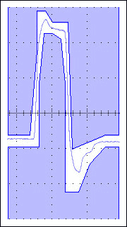
Referring to Figures 1 and 2, we can see that as the number of boards N in a N+1 redundancy implementation increases so does the maximum parallel off-capacitance that the backup board transceiver will observe. This parallel capacitance will have some effect on the output pulse shape and in the return loss performance. On the other hand, in normal operation (backup board inactive), the switch on-capacitance is the predominant capacitance the transceiver will see and this (smaller) capacitance is easily handled.
For good performance with the worst case capacitive loading condition (backup board active) it is recommended that the number N does not exceed 8 (1:8 redundancy protection). Figures 3 through 5 show the measured T1/E1 output pulses.
| T1, 0ft to 133ft LBO, 0ft cable, Normal Operation (1) | T1, 0ft to 133ft LBO, 0ft cable, N = 8 (2) |
|
(1) Output pulse through two series switches in the transmit path. |
(2) Output pulse from backup board with 8+1 configuration. |

| E1, Coaxial Cable, Normal Operation (1) | E1, Coaxial Cable, N = 8 (2) |
|
(1) Output pulse through two series switches in the transmit path. |
(2) Output pulse from backup board with 8+1 configuration. |


| E1, Twisted Pair Cable, Normal Operation (1) | E1, Twisted Pair Cable, N = 8 (2) |
|
(1) Output pulse through two series switches in the transmit path. |
(2) Output pulse from backup board with 8+1 configuration. |


Related to this Article
Products
T1/E1/J1 Single-Chip Transceiver
0.8-Ohm, Low-Voltage, Single-Supply SPDT Analog Switch in SC70
Product Categories
{{modalTitle}}
{{modalDescription}}
{{dropdownTitle}}
- {{defaultSelectedText}} {{#each projectNames}}
- {{name}} {{/each}} {{#if newProjectText}}
-
 {{newProjectText}}
{{/if}}
{{newProjectText}}
{{/if}}
{{newProjectTitle}}
{{projectNameErrorText}}
Latest Media 21


