Power Supply Modulation Ratio Demystified: How Does PSMR Differ from PSRR?
Power Supply Modulation Ratio Demystified: How Does PSMR Differ from PSRR?
by
Peter Delos
Dec 1 2018
Abstract
Many radar systems require low phase noise to maximize clutter rejection. High performance radars demand careful attention to phase noise, leading to significant design investment in lowering phase noise of synthesizers and characterizing the phase noise of synthesizer components.
Low phase noise performance—in particular, ultralow phase noise performance—is known to require low noise power supplies to achieve the best performance. What is not well documented is a systematic approach to quantify the impact of power supply noise voltage levels on phase noise. This article aims to change that.
The theory of the power supply modulation ratio (PSMR)—a measure of how power supply imperfections are modulated onto the RF carrier—is presented. An RF amplifier is characterized by, and measured results demonstrate that, the power supply noise contribution to phase noise can be calculated and fairly accurately predicted. Based on the result,a systematic approach for power supply specification is also discussed.
Introduction and Definition
The power supply modulation ratio is analogous to the well-known term power supply rejection ratio (PSRR), but differs by a key point. PSRR is a measure of how much the power supply imperfections are directly coupled to a component’s output. PSMR is a measure of how power supply imperfections of ripple and noise are modulated onto an RF carrier.
The Theory section below introduces H(s), a transfer function relating PSMR to power supply imperfections—how they are quantifiably modulated onto the carrier. H(s) has both amplitude and phase components, and can vary as a function of frequency and component operating conditions. Despite the number of variables, once characterized, the power supply modulation ratio can be used to accurately predict phase noise and spurious contributions from power supply based on supply data sheet specifications of ripple and noise.
Theory
Consider ripple on the dc power supply for an RF component. Supply ripple is modeled as a sine wave signal with a peak-to-peak voltage centered about the dc output. The sine wave is modulated onto the RF carrier, creating spurious signals at frequency offsets equal to the sine wave frequency.

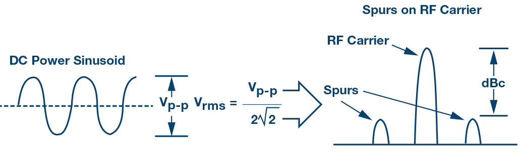
Figure 1. Sine wave ripple on a power supply modulates onto the RF carrier to create spurious signals.
The level of the spurs is a function of both the sine wave amplitude and the sensitivity of the RF circuit. The spurious signal can be broken down further into both an amplitude modulated component and a phase modulated component. The total spurious power level equals the spur power from the amplitude modulated (AM) component plus the spur power from the phase modulated (PM) component.
For the discussion here, H(s) is the transfer function from the power supply imperfections to an unwanted modulation term on the RF carrier. H(s) also has AM and PM components. The AM component of H(s) is Hm (s) and the PM component of H(s) is H∅ (s). The following equations make use of H(s) for practical RF measurements, with the assumption of low levels of modulation acceptable for power supply impact on an RF carrier.
Amplitude modulation of a signal can be written as
The amplitude modulation component m(t) can be written as
where fm is the modulation frequency
The AM modulation level of the RF carrier can be directly related to the power supply ripple by
vrms is the rms value of the ac component of the power supply voltage. Equation 3 is the critical equation that provides a mechanism to calculate the AM modulation of the RF carrier due to power supply ripple.
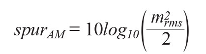
The spurious level can be calculated from the amplitude modulation by
The power supply impact to phase modulation can be similarly written. A phase modulated signal is
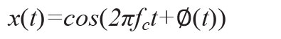
The phase modulated term is
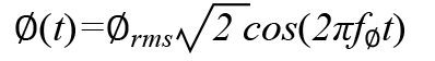
Again, the phase modulation can be directly related to the power supply by
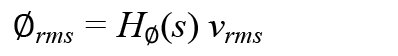
Equation 7 provides a mechanism to calculate the PM modulation of the RF carrier due to power supply ripple. The spurious level due to phase modulation is

To help visualize the spurious impact of mrms and ∅rms, a plot of the spurious level vs. mrms and ∅rms is shown in Figure 2.

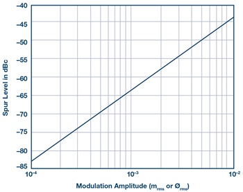
Figure 2. Spurious level vs. mrms and ∅rms.
To summarize this discussion, ripple on the power supply translates to modulation terms mrms and ∅rms from a sine wave rms voltage on the power supply of vrms. Hm (s) and H∅ (s) are the transfer functions from vrms to mrms and ∅rms, respectively.
Now, consider phase noise. Just as a sine wave modulates onto the carrier to create spurious signals, a 1/f voltage noise density modulates onto the carrier to create phase noise.

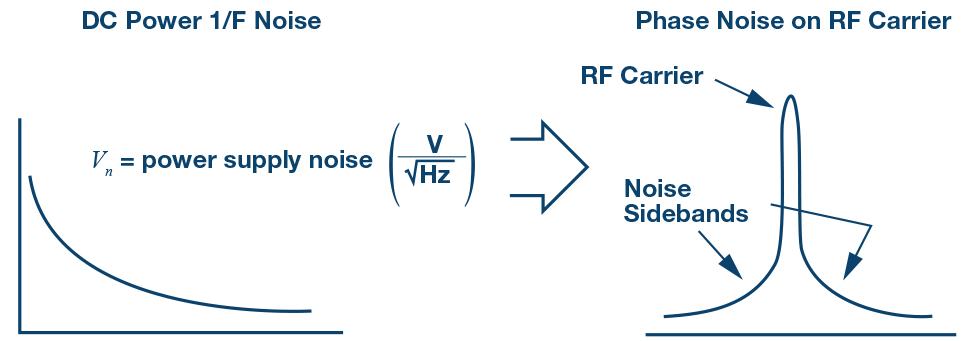
Figure 3. 1/f noise on a power supply modulates onto the RF carrier to create phase noise.
Again, if we consider a signal x(t) with a phase modulation, then
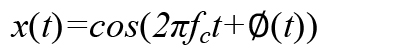
In this case ∅(t) is a noise term.
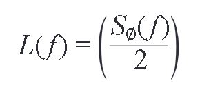
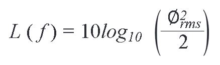
The power spectral density is defined as
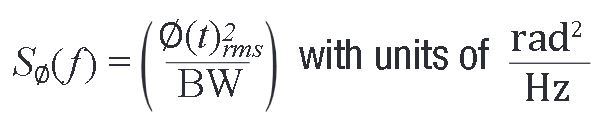
Phase noise is defined from the power spectral density as
Next, the same H∅ (s) used for spurs produced from phase modulation created from power supply ripple is applied to phase noise. In this case H∅ (s) is used to calculate phase noise from 1/f noise on the power supply.

A Measured Example
To demonstrate these principles, the HMC589A RF amplifier was characterized for power supply sensitivity and phase noise by measuring these quantities using several power supplies. The HMC589A evaluation circuit used for the characterization is shown in Figure 4.

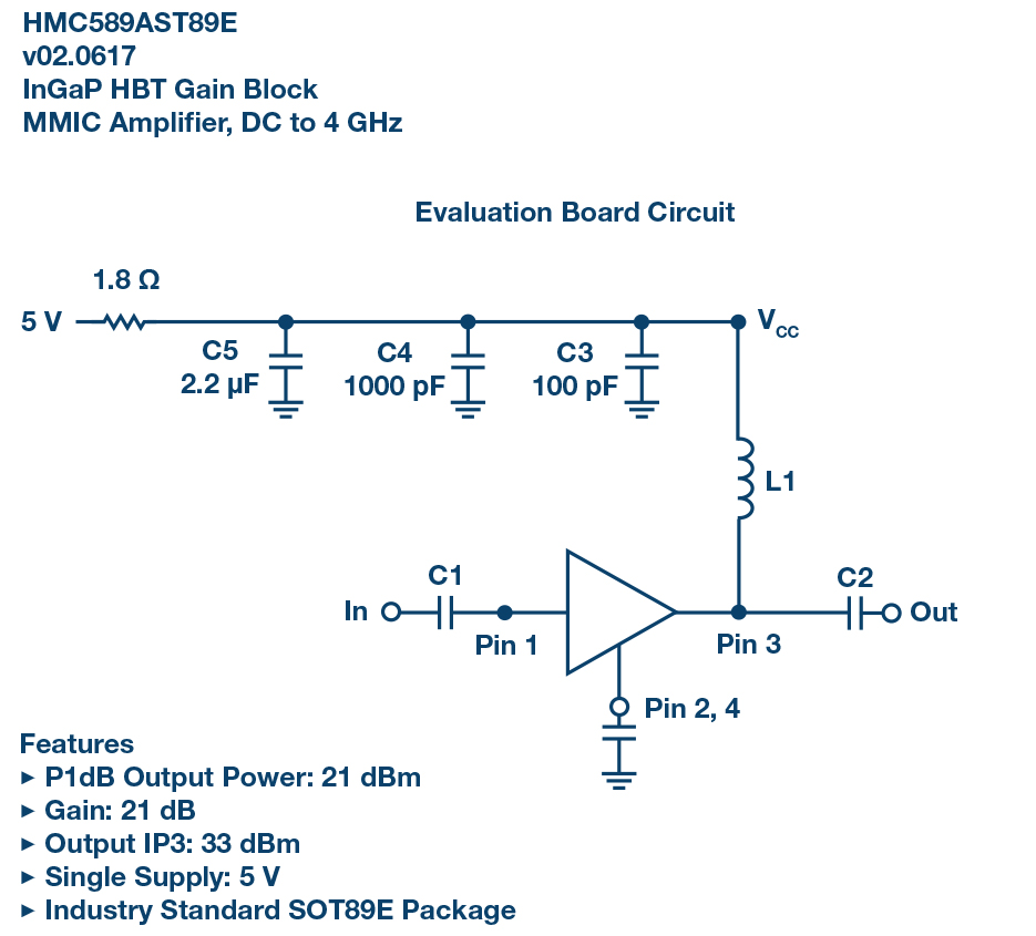
Figure 4. An HMC589A amplifier was used to demonstrate the PSMR principles.
To characterize the power supply sensitivity, a sine wave was injected onto the 5 V supply. The sine wave created spurious on the RF and the spurious signals were measured in dBc. The spurious content was further decomposed into an AM component and a PM component. A Rohde & Schwarz FSWP26 phase noise analyzer and spectrum analyzer was used. The AM and PM spur levels were measured through AM and PM noise measurements, respectively, with the spurious measurement enabled. Results are tabulated in test conditions at 3.2 GHz with an RF input of 0 dBm.
| Input Sine Wave | Measured Spurs | Calculated H(s) | |||||
| Frequency | V (rms) | Spur (dBc) | Spur (dBc) AM | Spur (dBc) PM | H (s) | H (s) AM | H (s) PM |
| 100 | 0.01 | –52.2 | –57.3 | –53.7 | 0.35 | 0.19 | 0.29 |
| 1000 | 0.01 | –52.4 | –57.2 | –54 | 0.34 | 0.20 | 0.28 |
| 10000 | 0.01 | –53.5 | –58.3 | –55.3 | 0.30 | 0.17 | 0.24 |
| 50000 | 0.0066 | –61 | –65 | –62.9 | 0.19 | 0.12 | 0.15 |
The test data demonstrated that the RF amplifiers power supply sensitivity can be empirically measured with a sine wave modulation and the results can be applied to predict power supply noise contribution to phase noise. More generally, this can be extended to any RF component; here we demonstrate the principles with amplifier characterization and measurements.
First, a rather noisy power supply was used. The noise density was measured. The power supply contribution to phase noise was calculated based on the characterized H∅ (s) and compared to the phase noise measurement. The Rhode & Schwarz FSWP26 was used for the measurement. The noise voltages were measured with a baseband noise measurement. The amplifier residual phase noise was measured with an additive phase noise measurement using the internal oscillator of the test set. The test configuration is shown in Figure 5. In this configuration, the oscillator noise is cancelled in the mixer, and any noise that is not common is removed in the cross correlation algorithm. This allows the user to achieve very lowlevel residual noise measurements.

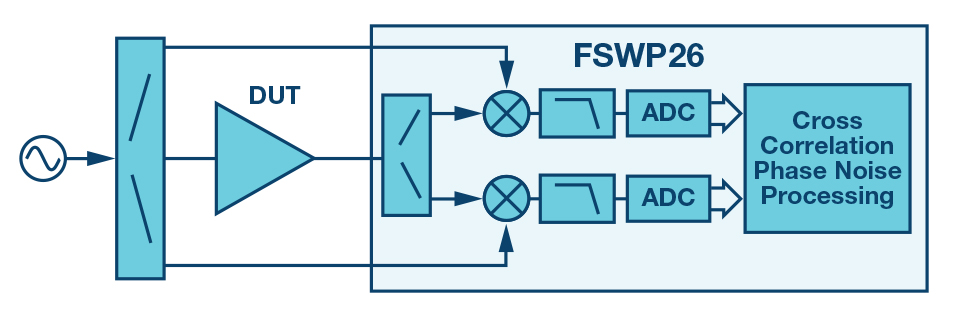
Figure 5. Amplifier residual phase noise test setup using the cross correlation method.
The power supply noise, measured phase noise, and predicted power supply noise contributions are shown in Figure 6. What becomes quickly apparent is the phase noise is dominated by the power supply between 100 Hz and 100 kHz offset, and the power supply contribution is accurately predicted.

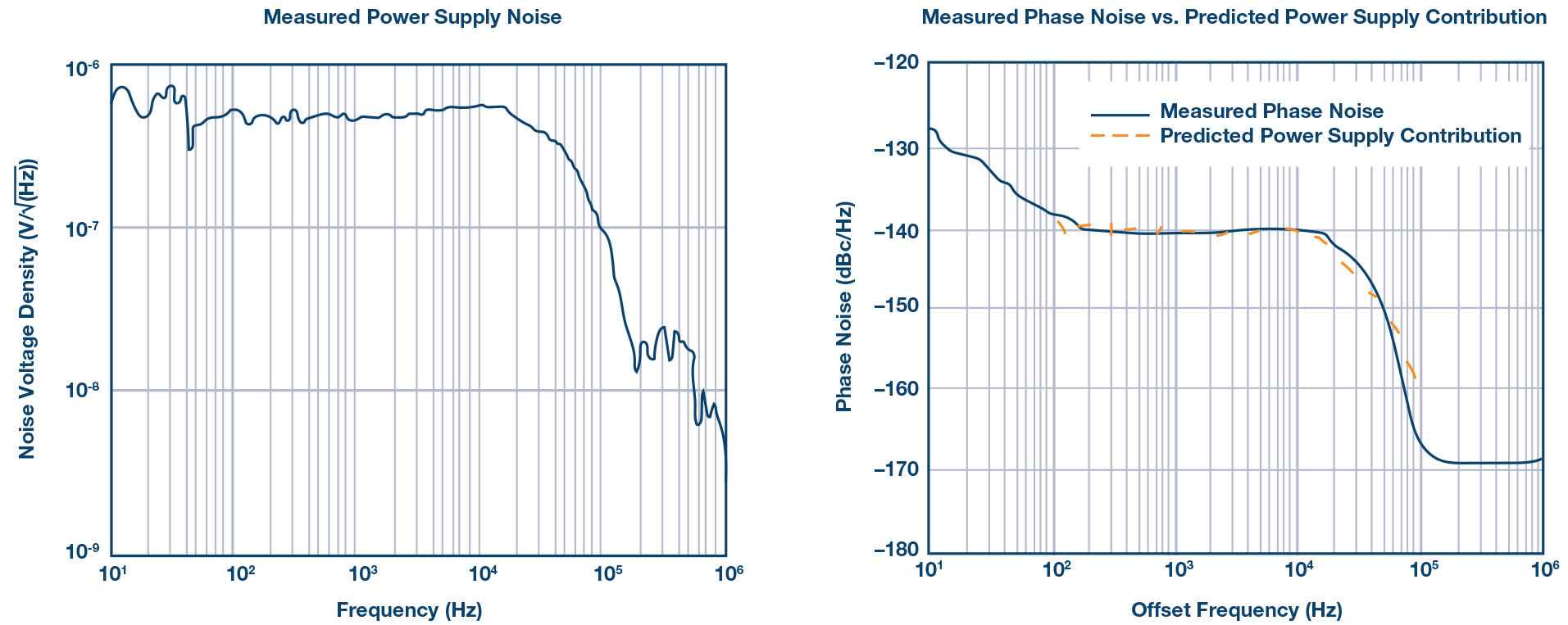
Figure 6. Validation of technique with a noisy power supply.
The test was repeated with two additional power supplies. The results are shown in Figure 7. Again, the power supply contribution to phase noise is remarkably predictable.

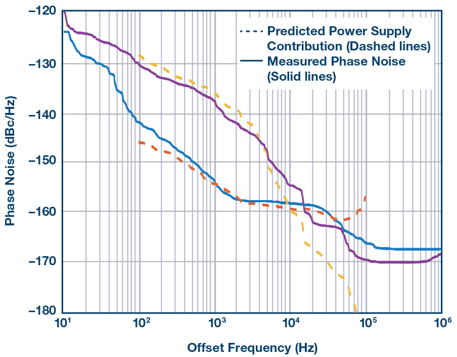
Figure 7. Validation of the technique with two additional power supplies.
A common challenge to low phase noise component characterization is ensuring the measurement is of the device and not the surrounding environment. To remove the power supply contribution from the measurement, an ADM7150 low noise regulator is used. The noise density quoted in the data sheet along with noise voltage measurements of the device used for the phase noise testing is shown in Figure 8.

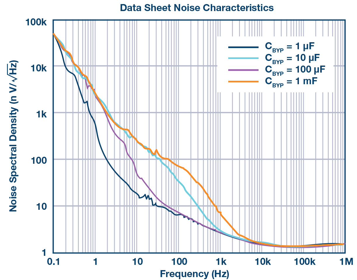

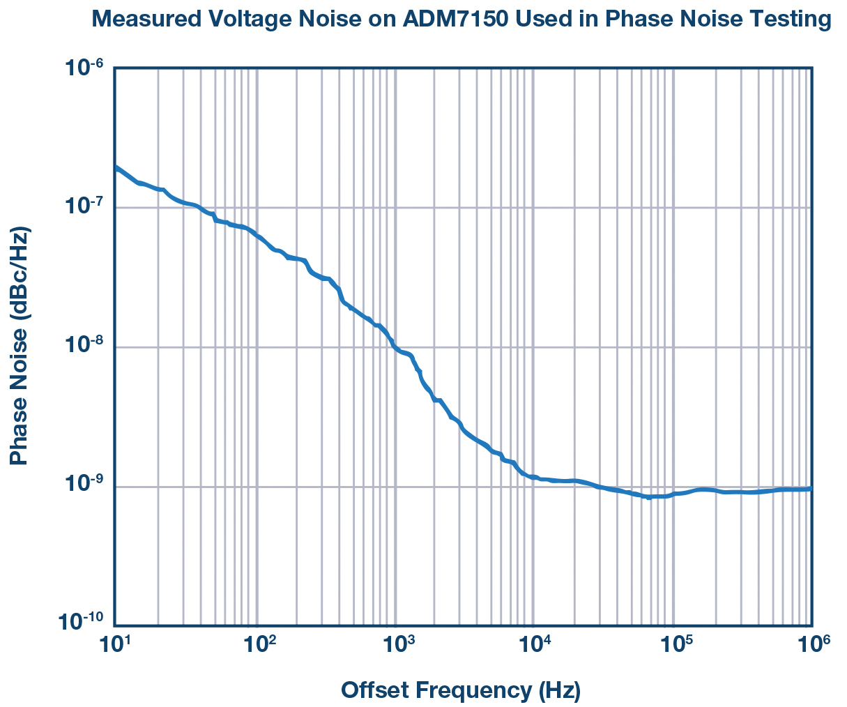
Figure 8. Low noise regulator ADM7150 noise voltage density.
A family of low noise regulators is shown in Table 2 with key parameters listed. The devices shown here are all well suited for powering RF components in low phase noise RF designs; consult the data sheets for conditions and characterization curves. In the data sheet, the noise density and PSRR curves are included across a number of offset frequencies. In the table, noise density is shown for the 10 kHz offset, as this region is typically a limiter for many regulators. PSRR is shown for the 1 MHz offset, as many linear regulators lose rejection capability at these offsets, requiring additional filtering.
| Part Number | VIN Range | VOUT Range | IOUT | Fixed/Adjustable | Noise Density @ 10 kHz | PSSR @ 1 MHz |
| LT3042 | 1.8 V to 20 V | 0 V to 15 V | 200 mA | Adjustable | 2 nV/√Hz | 79 dB |
| LT3045, LT3045-1 | 1.8 V to 20 V | 0 V to 15 V | 500 mA | Adjustable | 2 nV/√Hz | 76 dB |
| ADM7154 | 2.3 V to 5.5 V | 1.2 V to 3.3 V | 600 mA | Fixed | 1.5 nV/√Hz | 58 dB |
| ADM7155 | 2.3 V to 5.5 V | 1.2 V to 3.4 V | 600 mA | Adjustable | 1.5 nV/√Hz | 57 dB |
| ADM7150 | 4.5 V to 16 V | 1.8 V to 5 V | 800 mA | Fixed | 1.7 nV/√Hz | >60 dB |
| ADP7156 | 2.3 V to 5.5 V | 1.2 V to 3.3 V | 1.2 A | Fixed | 1.7 nV/√Hz | 60 dB |
| ADP7157 | 2.3 V to 5.5 V | 1.2 V to 3.3 V | 1.2 A | Adjustable | 1.7 nV/√Hz | 55 dB |
| ADP7158 | 2.3 V to 5.5 V | 1.2 V to 3.3 V | 2 A | Fixed | 1.7 nV/√Hz | 50 dB |
| ADP7159 | 2.3 V to 5.5 V | 1.2 V to 3.3 V | 2 A | Adjustable | 1.7 nV/√Hz | 45 dB |
The results of the HMC589A residual phase noise test when powered from the ADM7150 are shown in Figure 9. This measurement shows the true performance of the amplifier where the noise floors are below –170 dBc/Hz and this performance holds all the way to a 10 kHz offset.

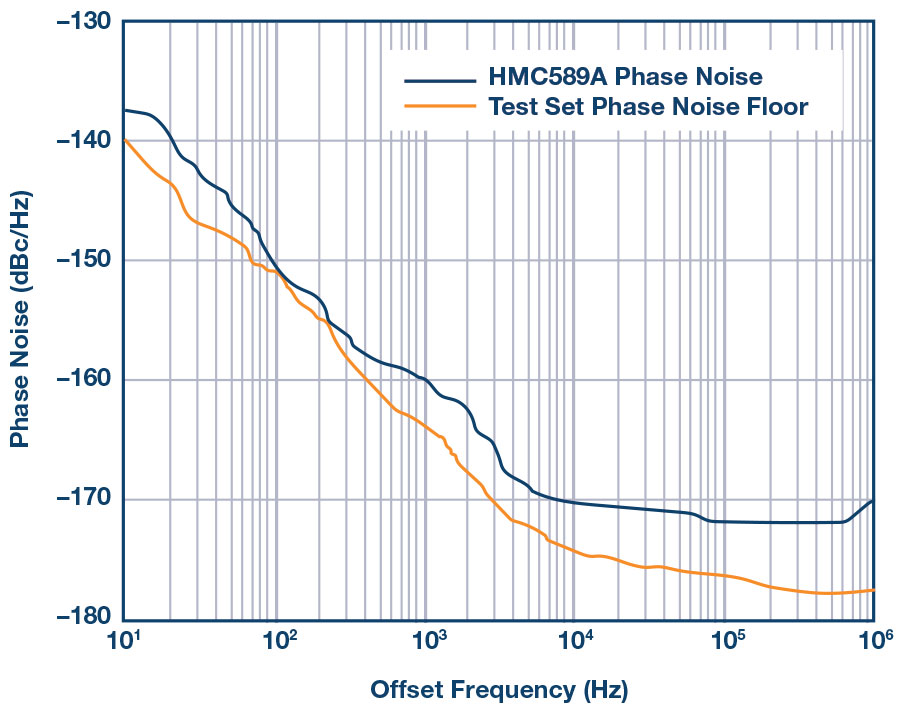
Figure 9. HMC589A residual phase noise at 3.2 GHz with a 0 dBm input RF power with dc power from the ADM7150 regulator.
A Systematic Approach to Power Supply Specification
Power supply design for low phase noise applications typically leads to cavalierly selecting the best regulation option available, disregarding actual minimal specifications, which leads to probable overdesign. For low volume designs this approach is likely worth continuing, but for high volume production, performance, costs, and complexity must be optimized—overdesign can be an unwelcome luxury.
Here is a method to quantitatively derive power supply specifications:
- Characterize H(s) with sine wave modulation on a power supply. H(s) will be a function of frequency, test every decade
- Allocate a power supply contribution to spurs and phase noise with some margin below the RF specification
- Calculate a power supply ripple specification,
- Calculate a power supply noise specification,
An important consideration in Step 1 above is an understanding of how Hm (s) and H∅ (s) vary under the operating conditions expected in the design. In the HMC589A characterization this variation was measured at several power levels and shown in Figure 10.


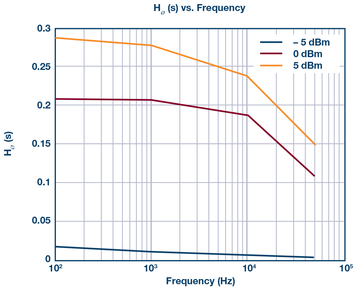
Figure 10. Variation of Hm (s) and H∅ (s) vs. offset frequency and power levels in the HMC589A evaluation circuit at 3.2 GHz.
Summary
Although it is generally accepted that power supply ripple and noise should be limited in RF applications, the quantitative impact is rarely, if ever, well understood. The systematic approach shown here enables the working engineer to make informed power supply choices by bringing discipline to the process of quantifying the impact of the power supply on desired RF performance.
About the Authors
Peter Delos is a technical lead in the Aerospace and Defense Group at Analog Devices in Greensboro, North Carolina. He received his B.S.E.E. degree from Virginia Tech in 1990 and M.S.E.E. degree from NJIT in 2004. Peter ha...
Related to this Article
Industry Solutions
Product Categories
Resources
{{modalTitle}}
{{modalDescription}}
{{dropdownTitle}}
- {{defaultSelectedText}} {{#each projectNames}}
- {{name}} {{/each}} {{#if newProjectText}}
-
 {{newProjectText}}
{{/if}}
{{newProjectText}}
{{/if}}
{{newProjectTitle}}
{{projectNameErrorText}}
Latest Media 21


