Abstract
Maxim serializers can connect and control camera ICs. This article describes how a camera's raw RGB or YUV output can be converted to RGB data that is suitable for use with a standard display.
Introduction
Maxim serializers can connect and control camera ICs. Such devices include the MAX9257, with a half-duplex UART/I²C control channel, and the MAX9259 and MAX9263, both with a full-duplex simultaneous control channel. The MAX9263 also supports high-bandwidth digital content protection (HDCP). This application note describes how a camera's raw RGB or YUV output can be converted to RGB data that is suitable for use with a standard display.
Camera Output Format
Camera chips, such as the OmniVision® OV10630, can be connected through a serializer. Interface pins for the OV10630 are pixel clock, PCLK, line valid, HREF, frame synchronization, VSYNC, and parallel data bits, D[9:0]. The data bits are stable at the rising edge of the clock.
Explanation of YUV and Raw RGB Formats
A CMOS camera sensor consists of millions of photo-sensitive cells. Each cell by itself reacts to light of all wavelengths. An optical-filter coating is used to make a particular sensor react only to red, green, or blue wavelength light. Adjacent cells are normally coated with colors in a Bayer arrangement, where twice as many cells are coated green, instead of red or blue. This mimics the physiology of the human eye. Taking sensor-cell outputs from left to right and from top to bottom, the raw RGB data is sequenced as Blue, Green...Blue, Green (end of the first line), Green, Red,...Green, Red (end of the second line), and so on, as shown in Figure 1.

Figure 1. Raw RGB data byte sequence.
RGB data that has the same density as the sensor cells can be produced by interpolating the desired colors from adjacent cells. Alternatively, this can be achieved by using colors of adjacent cells, in accordance with certain rules. One such rule for forming an RGB set for each pixel location is to use a pair of adjacent cells on the same line, plus the cell from the next (or previous) line next to the green. The interpolated RGB data is sequenced as..., Red(i-1), Green(i-1), Blue(i-1), Red(i), Green(i), Blue(i), Red(i+1), Green(i+1), Blue(i+1),... as shown in Figure 2. A set of RGB data for each pixel is needed to drive a color display while maintaining the maximum possible resolution of a camera sensor. The luminance resolution of such interpolated RGB data is close to that of the sensor cells, while the chrominance resolution is poorer. The perceived resolution can be as high as that of the sensor cells, since the human eye is more sensitive to the intensity of each pixel than to a pixel's color components.
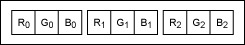
Figure 2. RGB data byte sequence.
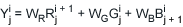
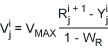
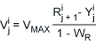
However, the data rate of such interpolated RGB data is tripled. To reduce the data rate, especially for transmission, the YUV color space (which fits an analog-color TV signal into a frequency band for an analog black-and-white TV) can be utilized. In the following equations, luminance is represented by Y, the color difference between blue and luminance is U, and the color difference between red and luminance is V,


where typical color weighting values are WR = 0.299, WB = 0.114, WG = 1 - WR - WB = 0.587, and normalization values are UMAX, and VMAX = 0.615.
For a camera sensor with a Bayer's pattern-color filter, either U or V data of adjacent pixels are about the same, depending on line-index i and pixel-index j (if the rule of using adjacent colors is utilized). Using this guideline, YUV data can be produced directly from raw RGB data, according to the following expressions.
 for even line-index i and even pixel-index j.
 for even line-index i and odd pixel-index j.
 for odd line-index i and even pixel-index j.
 for odd line-index i and odd pixel-index j.
 for even line-index i and even pixel-index j.
 for even line-index i and odd pixel-index j.
 for odd line-index i and even pixel-index j.
 for odd line-index i and odd pixel-index j.
 for even line-index i and even pixel-index j.
 for even line-index i and odd pixel-index j.
 for odd line-index i and even pixel-index j.
 for odd line-index i and odd pixel-index j.
To reduce the data rate, the even pixel-index U data and odd pixel-index V data are used, along with both even and odd pixel-indexed Y data. Such data rate reduced YUV data is transmitted in a sequence as shown in Figure 3. In other words, Y1, U0, and V1 are data for pixel 1; Y2, U2, and V1 are data for pixel 2, etc.

Figure 3. YUV422 data byte sequence.
The 422 indicates the sample ratio of Y:U:V. The 4:x:x standard was adopted due to the very earliest color NTSC standard, which used a chroma subsampling of 4:1:1, so that the picture carried only a quarter as much resolution in color than it did in brightness. Today, only high-end equipment processing uncompressed signals uses a chroma subsampling of 4:4:4 with identical resolution for both brightness and color information.
Serializer Input Format
The parallel interface of Maxim serializers is designed for 24-bit RGB data. Specifically, the MAX9259 has a pixel clock bit (PCLK) and 29 data bits that can be used for 24 RGB bits plus horizontal synchronization, vertical synchronization, and 3 control bits. In addition to the data parallel interface, the DRS and BWS pins need to be set to high or low for data rate and bus-width selections, respectively.
Maxim Serializers/Deserializers
The MAX9257 and MAX9258 serializer/deserializer (SerDes) pair has up to 18 parallel input/output bits suitable for transmitting YUV data, while the MAX9259/MAX9260 chipset has 28 parallel input/output bits suitable for transmitting RGB data. Another SerDes pair, the MAX9263/MAX9264, has 28 bits with added HDCP capability. In addition, the MAX9265 and MAX9268 is a SerDes pair of 28 bits with a camera link instead of a parallel input/output interface. All 28-bit Maxim serializers and deserializers have the same parallel-serial data mapping and can be used interchangeably. For example, a MAX9259 serializer can be used in conjunction with a MAX9268 deserializer to send RGB data (with the help of an FPGA). This data is sent from a CMOS camera over a serial link to a camera-link-interfaced display device.
Mapping of the Serializer
To match the camera link-output interface of the MAX9268 deserializer, the parallel RGB bits should be mapped according to the following signal diagrams. Figure 4 shows the mapping between the intermediate parallel bits of MAX9268 and its camera link output. Figure 5 shows the RGB content bit-mapping of the camera link. Table 1 shows the corresponding content mapping for the MAX9259 serializer.

Figure 4. The MAX9268 internal parallel-to-output mapping.

Figure 5. Camera link content mapping.
| DIN0 | DIN1 | DIN2 | DIN3 | DIN4 | DIN5 | DIN6 | DIN7 | DIN8 | DIN9 |
| R0 | R1 | R2 | R3 | R4 | R5 | G0 | G1 | G2 | G3 |
| DIN10 | DIN11 | DIN12 | DIN13 | DIN14 | DIN15 | DIN16 | DIN17 | DIN18 | DIN19 |
| G4 | G5 | B0 | B1 | B2 | B3 | B4 | B5 | HREF | VSYNC |
| DIN20 | DIN21 | DIN22 | DIN23 | DIN24 | DIN25 | DIN26 | DIN27 | DIN28 | |
| R6 | R7 | G6 | G7 | B6 | B7 |
Color Conversion: YUV to RGB
A FPGA chip can convert the data-rate reduced YUV data from the camera to RGB data for the MAX9259 serializer. The formula for this color-space conversion can be described by the following expressions when implemented in fixed-point math operation of 8 bit. n is even numbers for Dn and En in 2nd and 3rd equations.
Cn = Yn - 16
Dn = Dn + 1 = Un - 128
En = En + 1 = Vn + 1 - 128
Rn = clip((298 × Cn + 409 × En + 128) >> 8)
Gn = clip((298 × Cn - 100 × Dn - 208 × En + 128) >> 8)
Bn = clip((298 × Cn × 516 × Dn + 128) >> 8)
where >> 8 means "shift bits to the right eight times" and clip means "only taking the last 8 bits."
FPGA Solution
Input Buffering
An input buffering circuit consisting of a counter, three registers, and some combination logic is used to convert the single byte clocked input to triple byte clocked output at a half of the input clock rate. The combination logic is used to only enable the corresponding register for each Y, U, and V byte respectively.
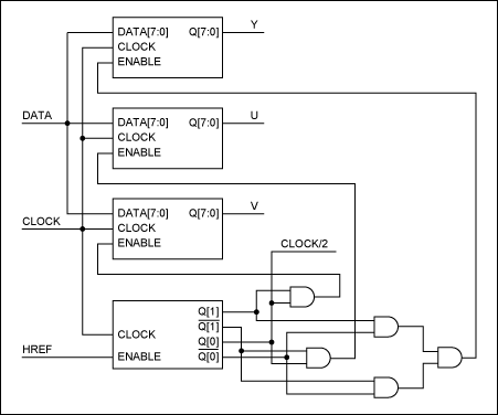
Figure 6. An input buffering circuit.
Clock Switch
FPGA output-pixel clock is one-half of the camera-pixel clock rate and drives the serializer pixel-clock input. However, the camera does not output the pixel clock before it has been initialized. The solution is to implement a 2-to-1 clock multiplexer (mux) and a clock-signal detector inside the FPGA. The mux is controlled by the clock-signal detector. The power-on default clock input of the mux is from the camera's clock oscillator, which makes the SerDes chipset provide the control channel to initialize the camera. The clock-signal detector counts the vertical-synchronization signal pulse. After a few vertical synchronization pulses, the mux switches to the half-rate of the camera-pixel clock. With a high-definition camera sensor like the OV10630, each period of one vertical-sync pulse contains much more than 100k pixel clocks. The time of a few vertical-sync pulses is enough to stabilize the camera's internal phase-locked loop (PLL). Counting vertical sync is much more efficient than counting pixel clocks and saves FPGA logic elements for the implementation.
Intermediate Buffering
The conversion expressions do not describe delays from hardware-circuit implementation. To produce RGB data from YUV inputs, two to three multiplications and three to four additions are required. Although an FPGA logic element (gate) only produces a few nanoseconds of delay, the propagations of carriers, adders, and shifted inputs of multipliers cause extensive delay and delay spread. To minimize the delay, each constant multiplier is approximated by an adder of two shifted inputs representing the 2 nonzero most significant bits (MSB) of the constant. Still at an input YUV byte rate of around 100MHz, the delay spread can cross timing boundaries of adjacent pixels, resulting to a noisy video. Intermediate registers to eliminate the delay spread are placed after every multiplier.
The aforementioned YUV-to-RGB color-space conversion has been implemented in an Actel® ProASIC3 A3PN125Z FPGA device. Figure 7 shows the schematic representation of this FPGA implementation.
|
|
|
| More detailed image. (PDF, 172kB) | More detailed image. (PDF, 180kB) |


Figure 7. FPGA implementation of the YUV-to-RGB converter.
Application Circuit
The camera chip can be provided on a daughter PCB by its vendor. Figure 8 shows the functional block diagram of a camera daughter module. The inputs are power supply, PWR, and crystal clock (XCLK). The output signals are parallel data bits (D0..D9), I²C bus (SDA, SCL), video synchronization (HREF, VSYNC), and pixel clock (PCLK).

Figure 8. Camera-module functional block diagram.
Figure 9 shows the schematic for the FPGA and serializer chips to complete the application circuits. The circuit is powered via the serial cable consisting of two twisted pairs of wires, one is used for the serial signal and the other for the power supply. Separate LDO power-supply ICs are used for the serializer and the FPGA devices. Bypass capacitors are used for the camera module, which has its own LDO supply chips, to further minimize potential interferences. Damping resistors are used for the data links between the FPGA and serializer devices.

More detailed image (PDF, 1.6MB)
Figure 9a. FPGA portion of the application circuit.

More detailed image (PDF, 1.6MB)
Figure 9b. Serializer portion of the application circuit.
MAX9259 is also capable of directly connecting to a camera sensor, like the OV10630, to build an even smaller camera head. The color-space converting FPGA can be used after the deserializer. Since this application needs a camera-link output, which can be directly driven by the MAX9268, the color-space converting FPGA is placed between the camera sensor and serializer (MAX9259).
Video Capture Example
Figure 10 shows the camera application-circuit implementation which is also captured using these camera application circuits.

Figure 10. Implementation of the camera-application circuit.
Summary and Future Direction
This application note describes a typical approach to use Maxim's camera serializer ICs in conjunction with an FPGA. The application schematic and FPGA code are available as an as-is design reference. RAW RGB to 24-bit RGB FPGA converter implementation will be available in a future update of this application note.
Related to this Article
Products
Gigabit Multimedia Serial Link with Spread Spectrum and Full-Duplex Control Channel
Gigabit Multimedia Serial Link Deserializer with LVDS System Interface
HDCP Gigabit Multimedia Serial Link Serializer with LVDS System Interface
HDCP Gigabit Multimedia Serial Link Serializer/Deserializer
HDCP Gigabit Multimedia Serial Link Serializer/Deserializer
Programmable Serializer/Deserializer with UART/I²C Control Channel
Gigabit Multimedia Serial Link with Spread Spectrum and Full-Duplex Control Channel
Programmable Serializer/Deserializer with UART/I²C Control Channel
Technology Solutions
Product Categories
{{modalTitle}}
{{modalDescription}}
{{dropdownTitle}}
- {{defaultSelectedText}} {{#each projectNames}}
- {{name}} {{/each}} {{#if newProjectText}}
-
 {{newProjectText}}
{{/if}}
{{newProjectText}}
{{/if}}
{{newProjectTitle}}
{{projectNameErrorText}}
Latest Media 20


