An Accurate Control Loop Model for Current-Mode Step-Down Controllers
Abstract
Peak current-mode control is preferred by power supply designers because it provides a first-order frequency response characteristic in the control-to-output transfer function. A control-loop design procedure based on the first-order model predicts a phase margin close to 90 degrees. It is found, however, that the phase margin obtained in practice is far less than 90 degrees depending on choice of crossover frequency, operating duty cycle, and amount of slope compensation used. This is due to the sampling effect of the control-loop current comparator. The following application note describes a control-loop design procedure for the MAX1954A current-mode controller that considers this sampling effect and accurately predicts phase margin. This analysis is not specific to the MAX1954A, however, and applies to most current-mode step-down ICs sold today.
The First-Order Model
A typical current-mode control loop for a step-down DC-DC converter is shown in Figure 1. A constant frequency clock, CLK, turns on the high-side MOSFET. Q1 turns off when the scaled-output inductor current at the inverting input of the PWM comparator exceeds the control voltage, vc. Thus vc programs the peak inductor current to maintain the output voltage, vo, constant. This results in a current source behavior for the output inductor, and therefore a first-order control-to-output transfer function. A compensating ramp, vs, is applied to a second inverting input of the PWM comparator to prevent subharmonic instability at duty cycles greater than 0.5 and to improve noise immunity. The relevant waveforms for current-mode control are shown in Figure 2.
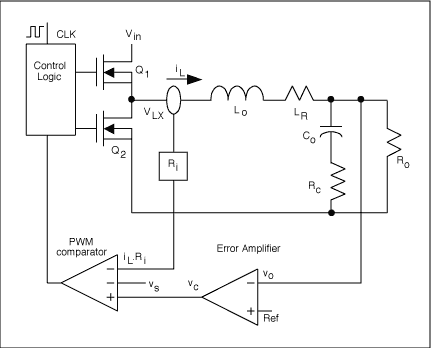
Figure 1. Peak current-mode control scheme.
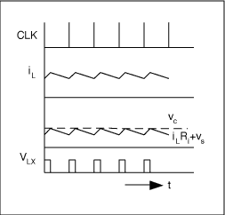
Figure 2. Current-mode control waveforms.
The control-to-output transfer function generally used for peak current-mode controller design is given in the following equation:
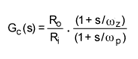
The above equation predicts a pole, ωp, due to the output capacitance, Co, and load resistance, Ro. The equation also predicts a zero, ωz, due to the output capacitance and its equivalent series resistance (ESR), Rc. The gain and phase predicted by the above model differ from that observed in practice because of the "sample and hold" effect in the PWM comparator that results from the current waveform getting sampled only once every cycle. It has been shown in [1] that the simple peak current-mode control model in the above equation must be modified to include a double pole at one half the switching frequency to account for the sampling effect.
Procedure for Predicting the Phase-Margin
Following is a description of a control-loop design procedure for the MAX1954A current-mode controller that considers this high-frequency effect and predicts the phase margin accurately. The MAX1954A evaluation kit circuit diagram is used to carry out the design. Both the MAX1954A evaluation kit data sheet and the MAX1954A data sheet are available.
The accurate control-to-output transfer function is given by the following equation:
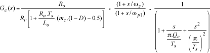
where duty cycle  , sampling effect quality factor
 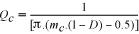 , slope compensation factor
  is the switching period, Se is the slope of the compensating ramp, if any, Ri is the product of the current-sense amplifier gain and current-sense resistance (high-side MOSFET Rds_on for the MAX1954A), Ro is the load resistance, Vo is the output voltage, and Vin is the input voltage. For the MAX1954A evaluation kit circuit, the following design parameters apply:
Vin = 11V
Vo = 1.5V
D = 0.136
mc = 1
Se = 0 (slope compensation applied at this duty cycle in the MAX1954A is negligible)
Ts = 3.3µS
Rc = 9mΩ
Co = 180µF
Lo = 2.18µH
Ro = 0.3125Ω
Ri = 0.063
The compensation network is designed as recommended in the MAX1954A data sheet. The control-to-output transfer function and the open-loop gain predicted by the accurate model are plotted using MathCad and are shown in Figure 3 and Figure 4 respectively. The actual control-to-output loop gain and open-loop gain transfer functions measured on the MAX1954A evaluation kit are shown in Figure 5 and Figure 6 respectively.
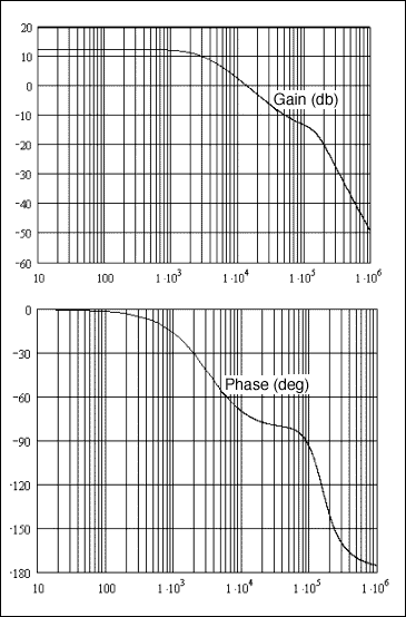
Figure 3.Control-to-output gain and phase plots from MathCad.
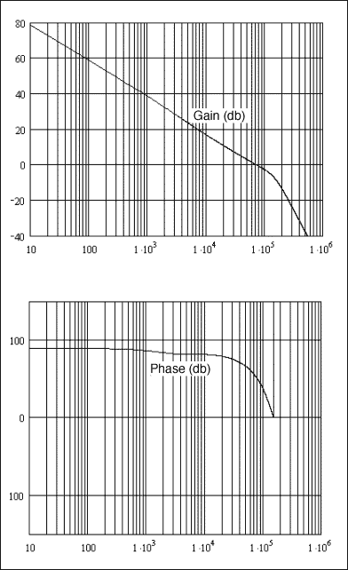
Figure 4.Open-loop gain and phase plots from MathCad.
Figure 5. Measured control-to-output gain and phase plots.
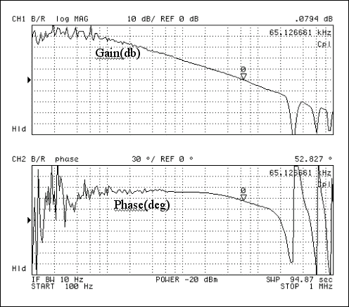
Figure 6.Measured open-loop gain and phase plots.
The control-to-output gain and phase predicted by the model match the measured values closely. At 101kHz, the model predicts -13.5db gain and a phase lag of -95 degrees. The measured plots show -15.1db gain and -88 degrees phase lag. The open-loop gain and phase plot from the model shows a crossover frequency of about 70kHz and a phase margin of 56 degrees. The measured plots show a crossover frequency of 65kHz and phase margin of 52.8 degrees. The first-order model would have predicted a phase margin of about 90 degrees, and may have implied that wider component tolerance was acceptable. To obtain the correct stability margins, therefore, a model that considers sampling effect is recommended even for peak current-mode designs with low crossover.
Related to this Article
Products
Product Categories
{{modalTitle}}
{{modalDescription}}
{{dropdownTitle}}
- {{defaultSelectedText}} {{#each projectNames}}
- {{name}} {{/each}} {{#if newProjectText}}
-
 {{newProjectText}}
{{/if}}
{{newProjectText}}
{{/if}}
{{newProjectTitle}}
{{projectNameErrorText}}
Latest Media 21


