ADC Driving: Driving Differential ADCs
For most fully differential applications, it is recommended that the LTC2389-18 be driven using the LT6201 ADC driver configured as two unity-gain buffers, as shown in Figure 1. The LT6201 combines fast settling and good DC linearity with a 0.95nV/√Hz input-referred noise density, enabling it to achieve the full ADC data sheet SNR and THD specifications, as shown in the FFT plot in Figure 2. This topology may also be used to buffer single-ended signals and achieves full ADC data sheet SNR and THD specifications in both pseudo-differential input modes, as shown in the FFT plots in Figures 3 and 4.

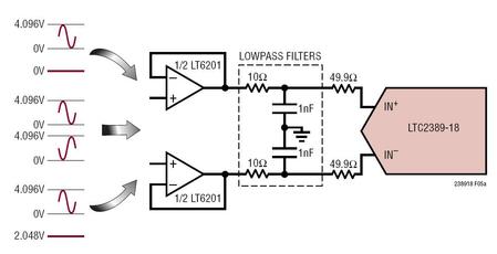
Figure 1. LT6201 Buffering a Fully Differential or Single Ended Signal Source

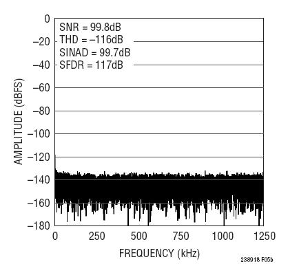
Figure 2. 32k Point FFT fSMPL = 2.5Msps, FIN = 2kHz, for Circuit Shown in Figure 1 Driven with Fully Differential Inputs


Figure 3. 32k Point FFT fSMPL = 2.5Msps, FIN = 2kHz, for Circuit Shown in Figure 1 Driven with Unipolar Inputs


Figure 4. 32k Point FFT fSMPL = 2.5Msps, FIN = 2kHz, for Circuit Shown in Figure 1 Driven with Bipolar Inputs
Single-Ended to Differential Conversion
In some applications it may be desirable to convert a single-ended unipolar or bipolar signal to a fully-differential signal prior to driving the LTC2389-18 to take advantage of the higher SNR of the LTC2389-18 in fully differential input mode. The LT6201 ADC driver configured in the topology shown in Figure 5 can be used to convert a 0V to 4.096V single-ended input signal to a fully-differential ±4.096V output signal. The RC time constant of the output lowpass filters is chosen to allow for sufficient transient settling of the LTC2389-18 analog inputs during acquisition. This wide filter bandwidth, coupled with the relatively high wideband noise of the single-ended to differential conversion circuit, limits the achievable SNR of this topology to 98.8dB, as shown in the FFT plot in Figure 6.

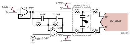
Figure 5. LT6201 Converting a 0V to 4.096V Single Ended Signal to a ±4.096V Fully Differential Signal


Figure 6. 32k Point FFT fSMPL = 2.5Msps, FIN = 2kHz, for Circuit Shown in Figure 5
An alternate single-ended to differential topology employing the LT6231 followed by the LT6201 is shown in Figure 7. This topology enables additional band-limiting of the wideband noise of the single-ended to differential conversion circuit using lowpass filters A without affecting the settling at the inputs of the LTC2389-18 during acquisition. This circuit achieves the full ADC data sheet SNR specifications, as shown in the FFT plot in Figure 8.

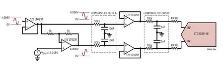
Figure 7. LT6231 Converting a 0V to 4.096V Single Ended Signal to a ±4.096V
Fully Differential Signal Followed by LT6201 Buffering Fully Differential Signal

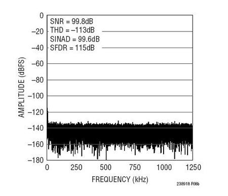
Figure 8. 32k Point FFT fSMPL = 2.5Msps, FIN = 2kHz, for Circuit Shown in Figure 7
Single-Ended Unipolar and Bipolar Inputs
The LTC2389-18 accepts both single-ended unipolar and single-ended bipolar input signals directly. For most single-ended applications, it is recommended that the LTC2389-18 be driven using the LT6200 ADC driver configured as a unity-gain buffer, as shown in Figure 9. The LT6200 combines fast settling and good DC linearity with a 0.95nV/√Hz input-referred noise density, enabling it to achieve the full ADC data sheet SNR and THD specifications in both pseudo-differential input modes, as shown in the FFT plots in Figures 10 and 11.


Figure 9. LT6200 Buffering a Single Ended Signal Source

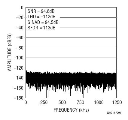
Figure 10. 32k Point FFT fSMPL = 2.5Msps, FIN = 2kHz, for Circuit Shown in Figure 9 Driven with Unipolar Inputs

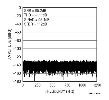
Figure 11. 32k Point FFT fSMPL = 2.5Msps, FIN = 2kHz, for Circuit Shown in Figure 9 Driven with Unipolar Inputs
Update
The LT6237 is an even better way to drive the LTC2389. The LT6237 is a low noise rail-to-rail output op amp with only 1.1nv/√Hz input referred noise voltage density that draws only 3.5mA and has a maximum offset voltage of only 315μV. This supply current and offset are considerably lower than that of the LT6201. The fully differential driver circuit is shown in Figure 12. Notice that while the time constant of the RC filter at the driver output is the same as that for the LT6201, the resistor has been made larger. SNR and THD performance are virtually identical to that of the LT6201 as shown in the FFT of Figure 13. Although the LT6236/7 has not been tested with the single-ended and single-ended to differential drivers shown earlier, performance should be similar to the LT6200/1. Just remember to change the filter portion of the circuit to incorporate the larger resistor and smaller capacitor values.

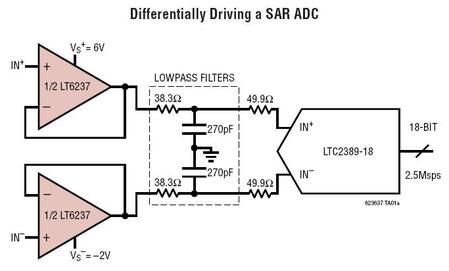
Figure 12. LT6237 Buffering a Fully Differential or Single Ended Signal Source

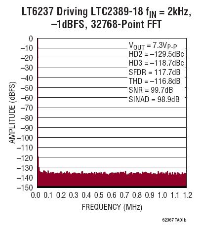
Figure 13. 32k Point FFT fSMPL = 2.5Msps, FIN = 2kHz, for Circuit Shown in Figure 12 Driven with Fully Differential Inputs
About the Authors
He began his career at LTC as a technician, learning from Bo...
{{modalTitle}}
{{modalDescription}}
{{dropdownTitle}}
- {{defaultSelectedText}} {{#each projectNames}}
- {{name}} {{/each}} {{#if newProjectText}}
-
 {{newProjectText}}
{{/if}}
{{newProjectText}}
{{/if}}
{{newProjectTitle}}
{{projectNameErrorText}}
Latest Media 21


