12A Monolithic Synchronous Buck Regulator Accepts Inputs up to 24V
12A Monolithic Synchronous Buck Regulator Accepts Inputs up to 24V
Jun 1 2007
Introduction
The LTC3610 is a high power monolithic synchronous buck regulator capable of providing up to 12A from inputs as high as 24V in a complete solution that takes little space (Figure 1). It integrates the step-down controller and power MOSFETs into a single, compact 9mm × 9mm QFN package. Its high step-down ratio, wide input and output voltage range and high current capability present a single IC solution for many applications previously requiring separate FETs and controller ICs. Its very low profile (0.9mm max) allows mounting on the back of a circuit board, freeing up valuable front-side board space.

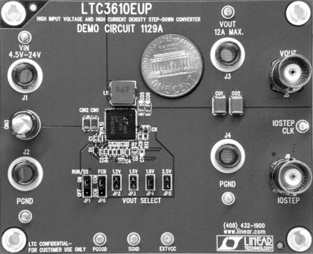
Figure 1. Who says a lot of space is needed for a complete high power density step-down regulator? The LTC3610 is capable of providing up to 12A from inputs as high as 28V. Its low 0.9mm profile allows it to be mounted on the back of the board too.
Flexible Control
High step-down ratios (Figure 2) are possible because of the LTC3610’s constant on-time operation and valley current control architecture, which allow a minimum on-time of less than 100ns. Output voltages approaching VIN are also possible (Figure 5). In either case, efficiency is very high—up to 97% (Figures 4 and 6). Synchronous operation affords high efficiency at low duty cycles, whereas a non-synchronous converter would conduct current through the forward drop of a Schottky diode most of the time. Transient response (Figure 3) is fast because the LTC3610 reacts immediately to a load increase. It does not wait for the beginning of the next clock cycle to respond, so there is no clock latency.

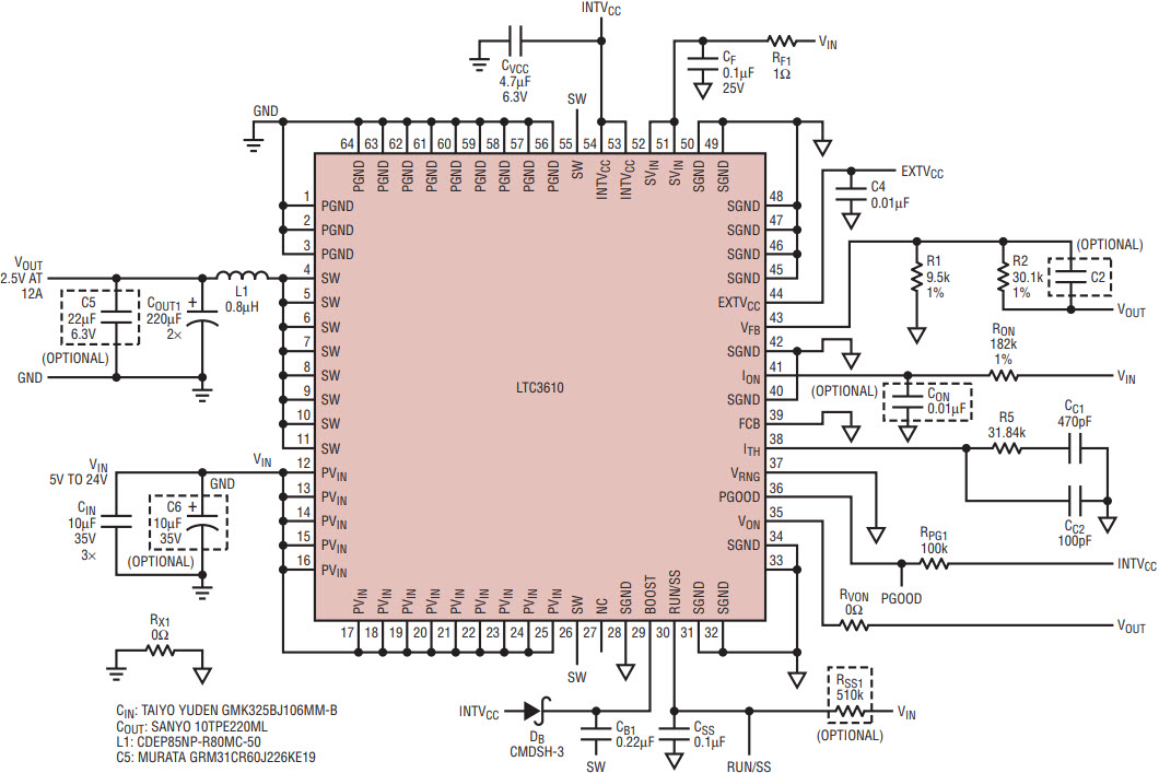
Figure 2. This converter runs at 550kHz and delivers 2.5V at 12A from an extremely wide 5V–24V input.

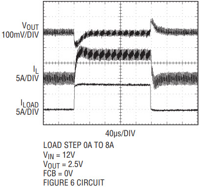
Figure 3. The LTC3610 responds quickly to an 8A transient (circuit of Figure 2).

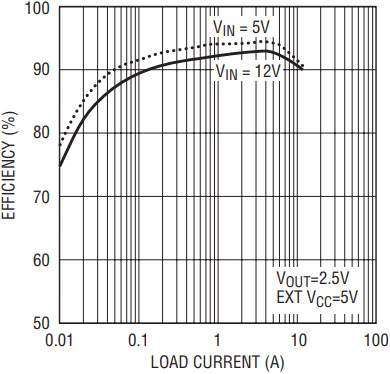
Figure 4. Efficiency vs load current for the circuit of Figure 2.

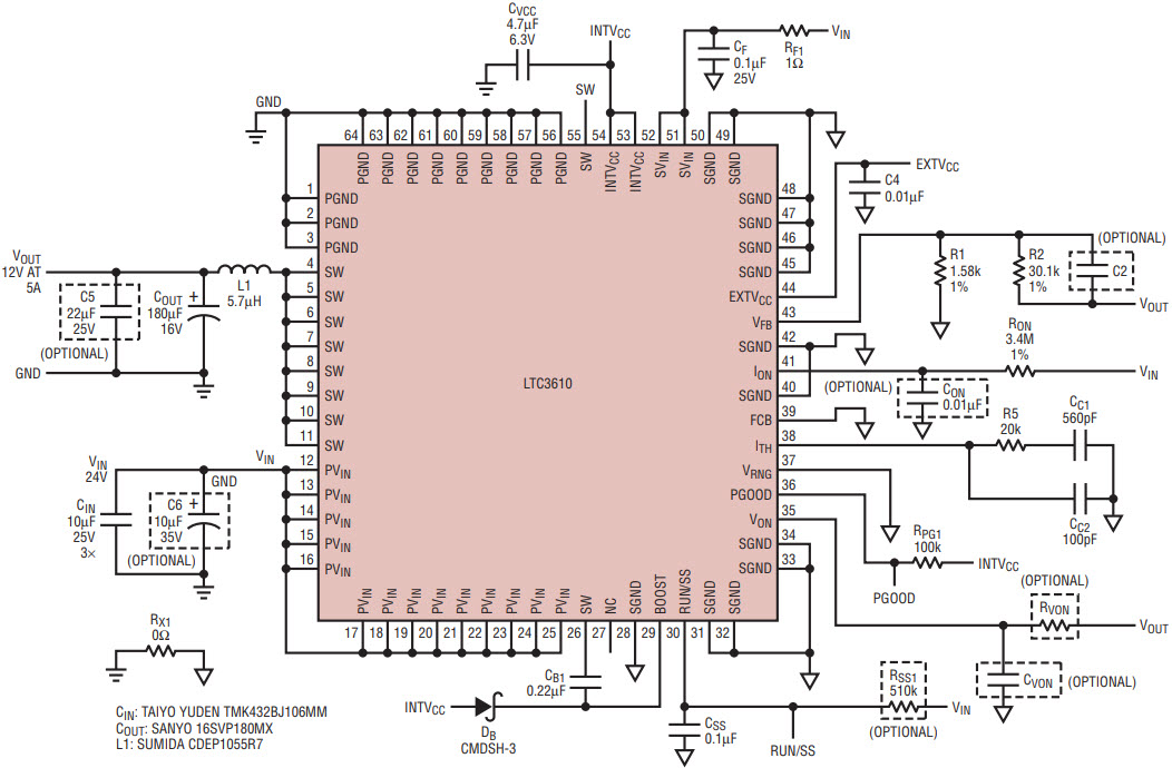
Figure 5. Although the LTC3610 is optimized for high step-down ratios, it can also regulate output voltages beyond the range of many DC/DC buck converters. For example, this schematic shows a 500kHz regulator delivering 12V at up to 5A, with high efficiency and low output ripple.

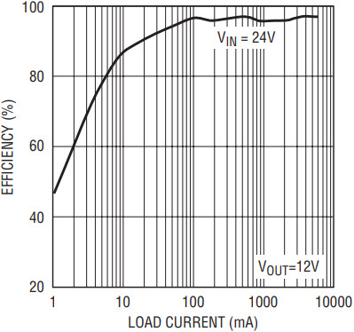
Figure 6. Efficiency vs load current for the circuit of Figure 4.
The LTC3610 can be programmed for two kinds of light-load operation: forced continuous mode or discontinuous mode. Forced continuous operation offers the lowest possible noise and output ripple. The top MOSFET turns on for the programmed on-time and the bottom MOSFET turns on for the (remaining) off-time. Inductor current is allowed to reverse, even at no load.
In discontinuous mode, the top MOSFET turns on for a preset on-time. Then (after a brief non-overlap period) the bottom MOSFET turns on until the current comparator senses reverse inductor current. When the error amplifier senses a small decrease at the feedback node VFB, its output (the ITH pin) rises, initiating another cycle. As the load current rises, so does the average inductor current. Eventually, the interval between constant on-time pulses ends before the inductor current can reach zero, at which point the inductor continuously conducts current. This point is determined by duty cycle, inductance value, and the interval between constant on-time pulses. By using single on-time pulses of fixed width, this mode provides well-controlled output ripple at any supported load. This process also prevents reverse inductor current, which minimizes power loss at light loads.
The on-time is set by the current into the ION pin and the voltage at the VON pin according to a simple equation

Tying a resistor RON from VIN to the ION pin yields an on-time inversely proportional to VIN.
Adjustable current limit is also built-in. The inductor current of LTC3610 is determined by measuring the voltage across the sense resistance between the PGND and SW pins, where RDS(ON) of the bottom MOSFET is about 6.5mΩ. The current limit is set by applying a voltage to the VRNG pin, which sets the relative maximum voltage across the sense resistance. An external resistive divider from the internal bias, INTVCC, can be used to set the voltage of the VRNG pin between 0.5V and 1V resulting in a typical current limit of 16A to 19A. Tying VRNG to SGND defaults the current limit to 19A.
The LTC3610 also has soft-start and latch off functions enabled by the Run/SS pin. Pulling the Run/SS below 0.8V puts the LTC3610 into a low quiescent current shut down state, whereas releasing the pin allows a 1.2µA current source to charge up the external soft-start capacitor. When the voltage on Run/SS reaches 1.5V, the LTC3610 begins operating with an initial clamp on ITH of approximately 0.9V. This prevents current overshoot during start up. As the soft-start capacitor charges, the ITH clamp increases, allowing normal operation at full load current. If the output voltage falls below 75% of the regulated voltage, then a short-circuit fault is assumed. At this point, a 1.8µA current discharges capacitor CSS. If the fault condition persists until Run/SS drops to 3.5V, the controller’s overcurrent latch off turns off the MOSFETS until Run/SS is grounded and released. If latch off is not desired, a pull-up current source at Run/SS defeats this feature.
Conclusion
Few synchronous monolithic DC/DC converters are versatile enough to use in low power portable devices such as notebook and palmtop computers, as well as high power industrial distributed power systems. The LTC3610’s broad input and output ranges, efficiency greater than 90% and high current capability make it a superior alternative to many solutions requiring separate power switches.
About The Authors
Related to this Article
{{modalTitle}}
{{modalDescription}}
{{dropdownTitle}}
- {{defaultSelectedText}} {{#each projectNames}}
- {{name}} {{/each}} {{#if newProjectText}}
-
 {{newProjectText}}
{{/if}}
{{newProjectText}}
{{/if}}
{{newProjectTitle}}
{{projectNameErrorText}}
Latest Media 21


