CN0590


Overview
Design Resources
Design & Integration File
- Schematic
- Bill of Materials
- Assembly Files
- Gerber Files
- Allegro Layout File
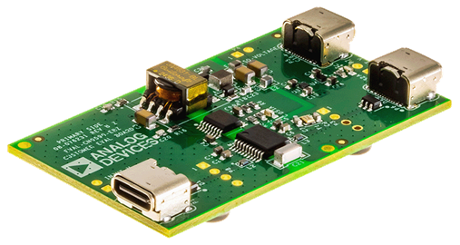
Evaluation Hardware
Part Numbers with "Z" indicate RoHS Compliance. Boards checked are needed to evaluate this circuit.
- EVAL-CN0590-EBZ ($107.00) EVAL-CN0590-EBZ
Features & Benefits
- USB 2 High Speed Isolated Retimer
- Type-C Connectivity
- Small Form Factor
- High Efficiency 2.5W Isolated Power
- Automatic Power Path Selectors with Integrated Protections for Optional External Power
Documentation & Resources
-
CN0590 User Guide (Wiki)4/17/2025WIKI
-
CN0590: Galvanic Isolation of USB High Speed Type-C Connector (Rev. 0)4/17/2025PDF841 K
Circuit Function & Benefits
Universal Serial Bus (USB) is an industry standard developed by USB Implementers Forum and is one of the most common point to point serial protocol interfaces. Historically, the USB protocol gained popularity in the industrial market providing a replacement for the RS-232 interface for debug and firmware upgrade. It emphasizes simple and robust connections between a host and a peripheral device, it is hot-swappable and offers USB power delivery. In particular, the USB 2.0 protocol is half-duplex and supports three communication speeds: 1.5Mbps (low speed), 12Mbps (full speed), and 480Mbps (high speed) which can allow fast data exchange.
Galvanic isolation can be used at the USB interface for functionality or safety reasons. Breaking ground loops while providing robustness to common-mode transients, together with a noise-immune connection are just few of the advantages of isolation integration which help to avoid signal integrity issues. Isolation can also be mandated by compliance to some safety standards such as the IEC 62368-1 for IT and A/V products, IEC 61010-1 for electrical equipment for measurement, control, and laboratory use, or IEC 60601-1 for medical equipment in industrial, instrumentation, energy, and medical applications to prevent fire or protect human operators against high voltage failures.
Type-C plugs and receptacles are gaining a lot of popularity and the reason is connected to their capability of supporting very high data rates, multiple protocols, smaller form factor, and their reversibility with respect to older legacy connectors such as Type-A or Type-B. Type-C connectors support the USB 2.0 PHY with the two standard pins: negative differential data line (DD-) and positive differential data line (DD+). This offers the possibility to use the advantages of the Type-C connectors for USB 2.0 communication.
The circuit shown in Figure 1 provides a plug and play USB 2.0 high speed isolator that can be used with any modern Type-C device supporting USB 2.0 connectivity. The CN0590 supports fully compatible output power and signal isolation up to 2.5W (500mA at 5V according to high-power hub port) and 480Mbps, respectively as specified in the USB 2.0 standard.

USB ISOLATION APPLICATIONS
USB ISOLATION FOR MEDICAL APPLICATIONS
In medical applications, isolation is critical for patient safety and is mandated by the IEC 60601 standard. Signal input ports (SIP) or signal output ports (SOP) are galvanically isolated to connect any off-the-shelf non-certified IT equipment to the medical device. Applied parts such as USB 2.0 cameras used in imaging systems or surgical applications also need to be galvanically isolated for patient safety.
Refer to the Common Variations section for guide on designing a Type-C USB 2.0 high-speed isolator that is suitable for medical applications.
USB ISOLATION IN INDUSTRIAL, ENERGY, AND INSTRUMENTATION APPLICATIONS
The USB 2.0 high-speed port is plug and play, hot swappable and allows fast data transfer. It is used in many applications for data logging, system debug and firmware upgrade as well as for connecting instruments and systems to PC for control, data visualization, and performing advanced measurements. Galvanic isolation in these applications is often mandatory to protect the human operator or systems from potential high voltage failure (floating or high voltage instruments cases), and the system from potential hazards such as common-mode transients and electrical noise by breaking harmful ground loops (often in industrial cases such as laptops near motor drives or welding machines). In the latter cases, galvanic isolation can prevent electromagnetic interference (EMI) from disrupting data transmissions and consequently avoid severe malfunctions. Isolation can also be useful in advanced high-end audio applications to enhance signal-to-noise ratio (SNR).
Circuit Description
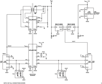
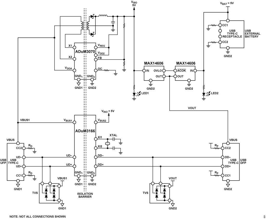
The CN0590 provides a completely isolated connection between a USB 2.0 host and a USB 2.0 device.
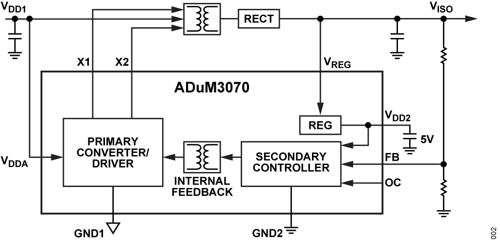
The design uses the ADuM3166 for USB 2.0 data isolation and the ADuM3070 driver with an external transformer for power isolation.
The system is rated up to 2.5kV rms isolation voltage per UL 1577 and features a system creepage and clearance (C&C) of 3.1mm limited by the ADuM3070 device. This system is suitable for functional isolation or basic and reinforced 300V rms Cat II isolation applications according to the IEC 61010 and IEC 62368 standard in many industrial, energy, and instrumentation applications. Consult the Common Variations section for higher isolation rating versions or more complex versions supporting isolated USB power delivery (PD) or isolated USB 2.0 hub applications.
The circuit in Figure 1 also provides an additional USB Type-C receptacle on the secondary side of the galvanically isolated barrier. This can be used to supply externally power-hungry loads needing more than 2.5W. Two MAX14606 handle the dual power source management by serving as power path selector, giving priority to the external supply in case present. These devices also serve as reverse polarity, overvoltage, and overcurrent protections for the circuit.
ISOLATED POWER
The CN0590 does not require external power to be operational. The USB Type-C input cable directly powers the isolators in the primary side of the isolators, while the isoPower® circuitry provides the necessary power for the secondary side.
The USB 2.0 standard requires the voltage supplied by high-power ports to be in the range of 4.75V to 5.25V (5V nominal). High-power ports must also be able to supply a minimum 500mA maximum current. The ADuM3070 is an excellent fit to meet these requirements.
Figure 2 shows the power isolation circuitry which uses the ADuM3070 isolator, a regulated DC-to-DC isolated power supply controller with an internal MOSFET driver. The ADuM3070 isolator provides a more stable output voltage and higher efficiency compared to unregulated isolated DC-to-DC power supplies. The fully integrated feedback and loop compensation in a small QSOP package provide a smaller form factor than any discrete solution. The ADuM3070 enables a DC-to-DC converter with an output voltage of 5.V, an output power of up to 2.5W (500mA), and up to an operating temperature of 105°C as specified in the USB 2.0 standard. Refer to the Circuit Performance section for the performance of the isoPower design in CN0590.

The USB Type-C connector includes some communication channel (CC) pins which are used for power negotiation. There are different power roles defined in the USB 2.0 standard namely: source (sources power to the bus), sink (sinks power from the bus), and dual role port (DRP). The CN0590 circuit note only focuses on sources and sinks. The CN0590 uses pull-up and pull-down resistors in the CC pins to identify the power roles in simple applications, such as the ones supported by this circuit note. Two pull-up resistors (RP) need to be connected from the CC pins to the VBUS voltage at the upstream connectors depending on the maximum power level the source can deliver. These not only indicate that the port is a source but also identify its power capability depending on the resistance value attached (see Table 1). Two pull-down resistors (RD) at the CC pins of the sink side connector indicate that the port is a sink.The value of the pull-down resistor is fixed and does notdepend on the power level since the sink is not able to provide power but can only sink power (except in DRP applications). Table 1 provides the values that shall be used for the implementation source’s pull-up resistor (RP) and sink’s pull-down resistor (RD). Refer to Type-C specifications for more information.
| Source Pull-up Resistor 4.75V to 5.5V | Sink Pull-down Resistor to Ground | Power Availability |
| 56kΩ ± 20% | 5.1kΩ ± 10% | Default: 900mA at 5V for USB 3.0 (4.5W), 500mA at 5V for USB 2.0 (2.5W) |
| 22kΩ ± 5% | 5.1kΩ ± 10% | 1.5A at 5V (7.5W) |
| 10kΩ ± 5% | 5.1kΩ ± 10% | 3.0A at 5V (15W) |
Sometimes, power hungry loads necessitate more than a USB 2.0 port can deliver. In this case, the third accessory Type-C port (P5) in CN0590 can be used to provide the extra necessary power (up to 15W, depending on the capability of the source attached). Two MAX14606 handle the dual power source management, while acting as power-path selectors. Refer to Common Variations section for options supporting power delivery or isoPower rating above 2.5W.
USB HIGH SPEED SIGNALING
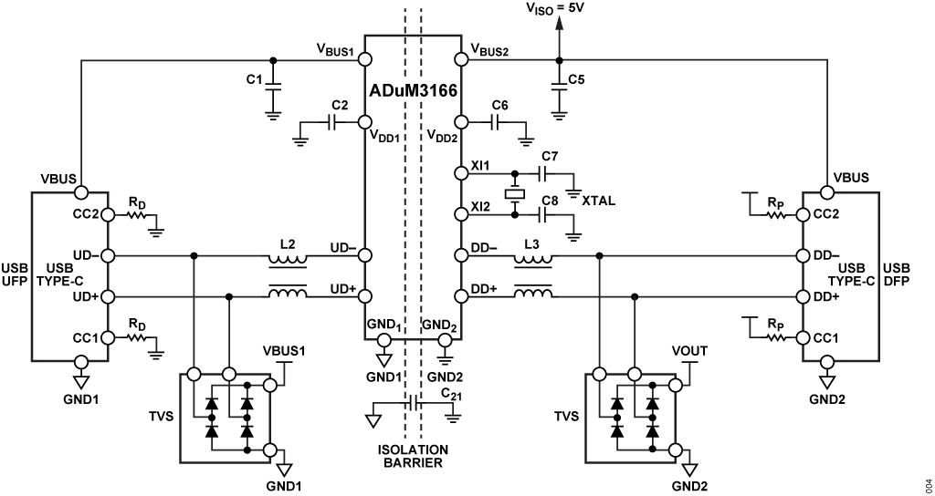
The CN0590 uses the ADuM3166 for the isolation of USB 2.0 high-speed signals. The ADuM3165/ADuM3166 are USB 2.0 port isolators, utilizing Analog Devices, Inc., iCoupler® technology to dynamically support all USB 2.0 data rates: low (1.5 Mbps), full (12 Mbps), or high (480 Mbps), as required. The devices support automatic speed negotiation. High-speed data is retimed to reset the jitter budget of the USB 2.0 communication link, ideally doubling the cable length reachable by the USB 2.0 standard (5m) and providing leading signal integrity for the harshest industrial environments. In order to retime the data, the ADuM3165/6 require an external clock signal or crystal input. The ADuM3165 supports the clock or crystal input on the upstream side, and the ADuM3166 supports the clock or crystal input on the downstream side, offering two options to best suit the system design in case the clock is provided by a processing unit and not by a crystal oscillator. For system designs where the clock is provided by an external crystal oscillator either device can be used. Refer to USB High Speed Eye Diagram Test section for additional details on the benefits of data retiming.
The USB 2.0 isolators also feature industry’s leading low power and compactness which provide space and power saving at the system level. The low-power standby mode for downstream side supports applications with limited available power, such as battery-operated peripherals. The upstream side standby current meets USB 2.0 requirements for suspended operation. The USB 2.0 isolators are specified over an extended industrial temperature range of −55°C to +125°C and are available in a compact 20-lead shrink small outline package (SSOP) with 5.3mm creepage and clearance.
EXTERNAL PROTECTIONS
USB ports get often in touch with humans and potentially harmful electrostatic discharges (ESD) that can damage the components, compromising the functionality of the circuitry. Transient-voltagesuppression (TVS) are often used to enhance the protection of the system against these types of events. When selecting TVS suppressors, the most important parameters to consider are ESD protection level, dynamic resistance, clamp voltage, input capacitance, and transmission line pulses (TLPs). In CN0590, the SRV05-4HTGD ESD suppressor diode array from Littlefuse was selected. This offers rugged ESD robustness up to ±30kV contact/air according to IEC 61000-4-2 with only 0.2Ω dynamic resistance and 1pF capacitance.
Electromagnetic compatibility (EMC) is of paramount importance when dealing with galvanic isolation. The two isolation barriers form a dipole antenna which can radiate. For this reason, a common- mode choke suitable for USB 2.0 communication has been added in series with the ADuM3166, together with a Y-Cap capacitor to short the dipole antenna preventing it from radiating. The CN0590 has a differential and common-mode filter added in series with the isoPower output to minimize conducted electromagnetic interference due to the isoPower (not shown in the simplified block diagram).
Figure 2 shows the overcurrent protection circuitry, which utilizes the MAX14606 for thermal management. A load switch is a good alternative to this device if more precise current protection is required. The MAX869L is a P-channel load switch featuring an accurate programmable trip current limit from 400mA up to 2.4A and low on-resistance so it is suitable for USB applications. This switch is designed to protect the power source from shorts and surges by limiting current. An alternative to this device is the MAX20333 featuring a programmable current-limit (from 0.2A up to 5.5A) to prevent damage to host devices due to faulty load conditions. This current limit switch features a low 23mΩ (typical) on-resistance and operate from a 3.5V to 22V input voltage range, so is suitable for power delivery applications up to 100W. Refer to the Load Switch and Digital Isolators for Overcurrent Management in USB 2.0 Isolated Hub Applications for more information on how to handle this device in an isolated USB port.
The accessory external Type-C port can come accidentally in touch with a higher voltage supply, potentially damaging the components in this circuit design. The CN0590 has an on-board MAX14606 to manage the input overvoltage and reverse current protections for such instances. The MAX14606 features low 54mΩ (typical) onresistance (RON) internal FETs and protects low-voltage systems against voltage faults up to +36V. When the input voltage exceeds the overvoltage threshold, the internal FET automatically turns off to prevent damage to the protected components. The MAX14606 is specified over the extended -40°C to +85°C temperature range and are available in 9-bump WLP packages.
CIRCUIT PERFORMANCE
COMMON-MODE TRANSIENT IMMUNITY
Common-mode transient immunity (CMTI) refers to the ability of an isolator to reject fast common-mode transients. The CMTI is defined as the maximum common-mode voltage slew rate or transient that can be tolerated between system ground (Ground 1) and isolated ground (Ground 2), while still maintaining bit error free communication.
CMTI is important because high slew rate transients can couple across the parasitic capacitance of the isolation barrier, corrupting data. The ADuM3070 and the ADuM3166 are robust digital isolators with good CMTI performance, specified to operate correctly and without data corruption in the presence of common-mode transients greater than 25,000 V/μs and 40,000 V/μs, respectively.
RADIATED EMISSIONS
Each of the components used in CN0590 passed the CISPR32 Class B.
The CN0590 isoPower design has provisions for external snubbers in case further EMI suppression is needed. Figure 3 shows the reference designators of the primary and secondary snubbers namely: R15, R16, C19, C20 (primary) and R17, R18, C22, and C23 (secondary).

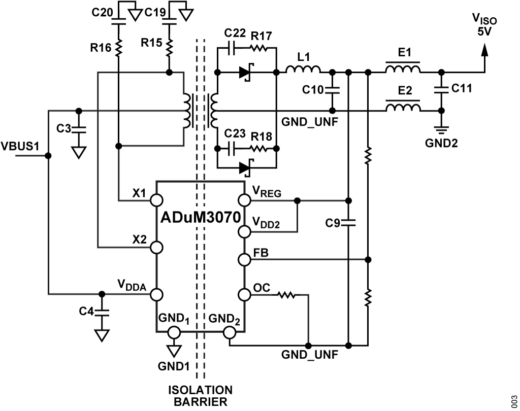
The E1 and E2 ferrite beads form a common-mode filter with C11 to help minimize radiated emissions. Note that the ground of ADuM3070 (GND_UNF) is different from the one of the downstream Type-C connector (GND2) and is marked as unfiltered ground (GND_UNF). This is to prevent conducted common-mode noise, coming from the isoPower circuitry, to couple with the downstream Type-C cable.
As illustrated in Figure 4, an external optional Y-Cap capacitor (C21) with a capacitance value of 100pF provides a low impedance path for common-mode currents . The L2 and L3 common-mode chokes have been added in series with the USB 2.0 lines to filter unwanted common-mode noise as well.

When implementing similar design, care must be taken in the selection of the Y capacitor in order for it not to affect the system creepage and clearance.
USB 2.0 POWER ISOLATION
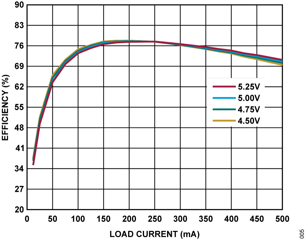
Figure 5 shows the CN0590 power isolation circuitry's typical efficiency compared to the load current and as measured at ambient temperature. The efficiency curve reaches a peak of about 78% at an output current of 200mA.

The plot in Figure 6 depicts the typical output voltage function vs. the load current. The results show a stable behavior for input voltages within the range specified by the USB 2.0 standard.

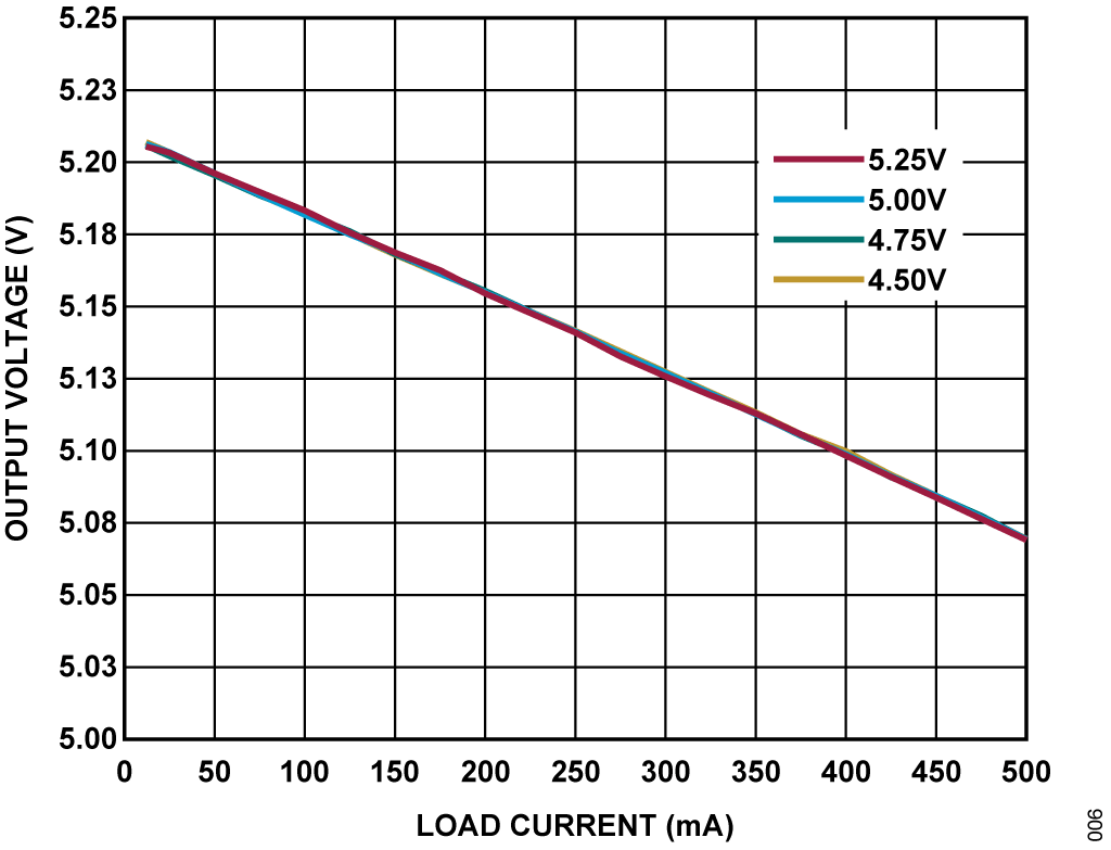
Both graphs are parametrized per input voltage of 4.5V, 4.75V, 5V, and 5.25V measured at the upstream facing the Type-C connector. The linearity depends on the parasitic resistance in series between the isoPower output and the USB Type-C connector, dominated by the common-mode choke and the power path selector.
USB HIGH SPEED EYE DIAGRAM TEST
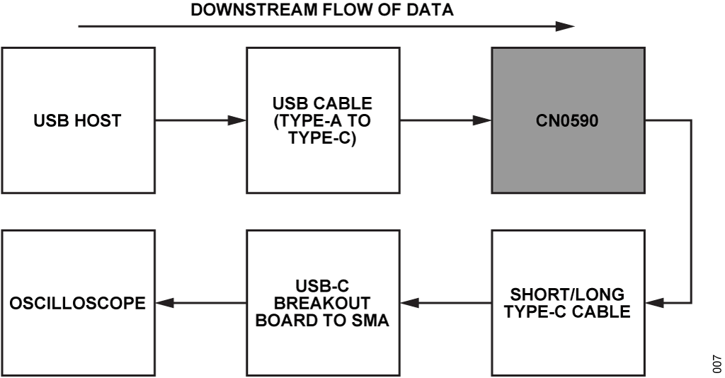
This subsection describes a USB 2.0 high-speed eye diagram test performed with the CN0590. Figure 7 illustrates the CN0590 complete test setup for evaluating downstream data flow.
The setup uses a USB host with a USB port to generate the USB high speed downstream data flow. The direction of the data is important in a half-duplex connection because determines what is transmitting and what is receiving.
The USB host generates a test packet by means of the USB-IF XHSETT software. The waveform captured by the oscilloscope in single acquisition mode is saved and uploaded in the USB-IF USBET20 tool to generate the eye diagrams.

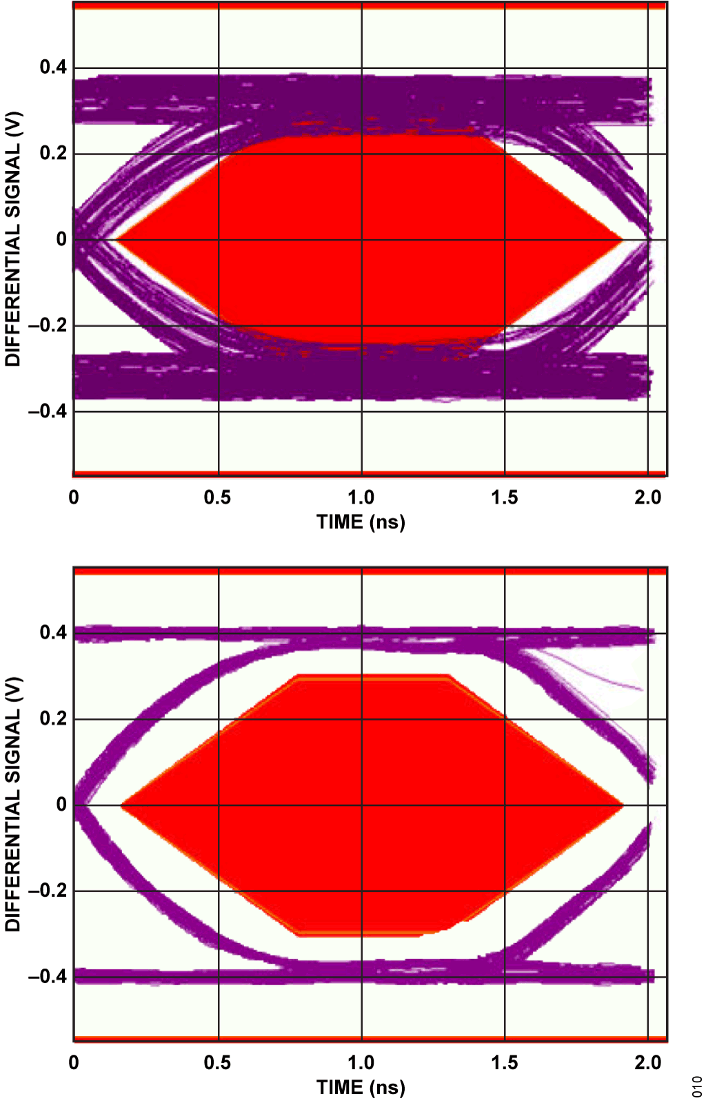
A near end mask is an eye diagram mask applicable for short channels. If the eye diagram hits the mask, it fails the test since a violation of timing requirements occurs. For this test, a very short cable was used in between the CN0590 and the breakout board to capture the samples and measure the eye diagram with the oscilloscope.

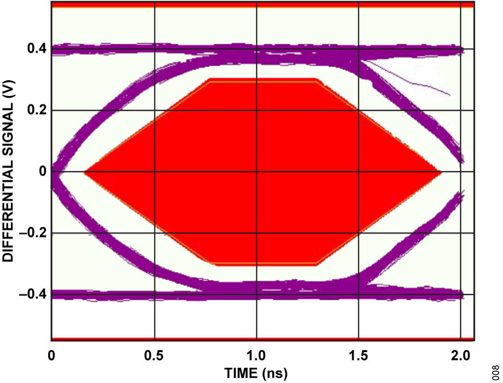
Figure 9 is an eye diagram with a far end mask applied. A far end mask, contrary to a near end mask, is an eye diagram mask applicable for long channels. For this test, a Type-C cable of 1 meter length has been used in between the CN0590 and the breakout board used to connect to the scope and capture the eye diagram. The effect of the 1 meter Type-C cable can be seen in a slight increase of the jitter and attenuation when this eye diagram is compared to the plot shown in Figure 8.

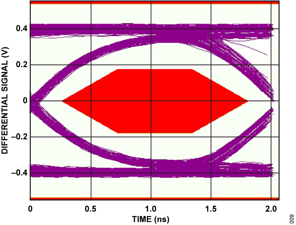
Figure 10 reveals the effects and benefits of retiming by comparing a USB 2.0 eye diagram taken with CN0590 and one without it. The eye diagram taken with the CN0590 has been captured with an upstream cable of 5 meters length, a downstream flow of data and a USB-IF fixture connected right to the secondary side of CN0590 board. It can be clearly observed that in the case where the USB 2.0 isolated retimer is used, the jitter is freed of any random and deterministic components coming from the USB 2.0 channel. This is made possible by the clock data recovery integrated in the ADuM3166, which resets the jitter budget of the USB 2.0 link. The isolated retimer not only acts on the eye width but also on the eye height, restoring typical USB 2.0 signal levels of 800 mVP-P

LAYOUT GUIDELINES
The layout in CN0590 is an integral part of the design and is key to achieving optimum signal integrity, efficient and low noise isoPower transfer, and effective external protection at the system level. Carefully following the layout guidelines in this section can prevent layout re-spins and debugging activities leading to faster development cycle and time to market.
- Route the USB 2.0 differential pairs (D+/D-) with a controlled differential impedance of Z0=90Ω ± 15% and a common-mode impedance of ZCM = 30Ω ± 30% per the USB 2.0 standard. A 4-layer printed circuit board (PCB) is mandatory for this reason.
- Avoid using vias in high-speed USB differential pairs since these can introduce impedance discontinuities. When vias are unavoidable, use return path vias to minimize the impedance discontinuities which can cause reflections, ultimately worsening signal integrity.
- Minimize the trace length between the ADuM3166 and the USB port or between the ADuM3166 and the host or device to minimize the resulting insertion loss which can cause intersymbol interference (ISI) jitter and eye diagram closure.
- Surround USB data lines with ground planes for crosstalk immunity and better shielding.
- Remove ground planes in the middle of the pads of commonmode chokes in series with USB data lines. These introduce parasitic series capacitance that minimize the effectiveness of the inductive choke.
- Maintain symmetry and short traces between the clock crystal and the ADuM3166 to balance and minimize capacitive and inductive parasitics. Surround the external crystal with a ground plane for shielding. The ground plane must also be placed in the layer below the crystal.
- Keep decoupling capacitors as close as possible to the device supply pins and complete routing within the same layer as the device to minimize the resulting parasitic inductance and avoid supply drops when the device is in USB 2.0 high-speed mode. The overall length of the traces connecting the decoupling capacitor to the leads of the package must be kept less than 5mm for this purpose.
- Place the external ESD suppressor very close to the Type-C connector and ensure a good connection to ground with multiple vias to offer a very good frequency response and minimize stray inductances. Generally, the ESD protection should be located as close as possible to the point of entry of expected electrostatic discharges, keeping a minimum PCB trace lengths to the power supply, ground planes, and between the IC device and the protection itself to minimize stray series inductance.
Common Variations
HIGHER ISOLATION RATING OPTIONS TO SUPPORT 5KV RMS & 8MM C&C APPLICATIONS
As regulated by the IEC 60601-1 standard, medical applications require a higher system creepage and clearance to support means of patient protections (1MOPP) at 250V rms for SIP and SOP ports and 2MOPP at the sum of secondary and patient voltage domains. This requires a minimum of 4mm of creepage and clearance and 1.5kV rms of isolation voltage which the ADuM3165/ADuM3166 can meet. The ADuM4070 is the alternative isoPower option to support higher creepage (see Alternative Power Options section). In case higher creepage is also needed at the USB data lines to meet higher 2MOPP or over voltage categories (OVC) ratings, the ADuM4165/6 features a minimum creepage and clearance of 8.3mm. Refer to Table 2 for guide on choosing appropriate parts to meet the minimum required isolation voltage and creepage and clearance at the system level.
| Isolation Rating | Functional and Basic | Reinforced |
| Minimum Isolation Voltage | 2.5kV rms | 5kV rms |
| Minimum Creepage | 3.1mm | 8mm |
| DC-to-DC Converter | ADuM3070 | ADuM4070/ LT8301/ LT8302 |
| USB 2.0 Isolators | ADuM3165/ADuM3166 | ADuM4165/ADuM4166 |
LOAD SWITCH AND DIGITAL ISOLATORS FOR OVERCURRENT MANAGEMENT IN USB 2.0 ISOLATED HUB APPLICATIONS
In some applications, such as USB 2.0 isolated hubs, the power flow at the USB 2.0 downstream port is controlled by the hub itself. Hubs can also stop power delivery in case an overcurrent detection occurs. USB hubs have a fixed upstream data rate while dynamic downstream data rates. This fits very well with the automatic speed negotiations feature of the ADuM3165/ADuM3166 and ADuM4165/ADuM4166 devices, which allow isolation to be seamlessly dropped in the downstream port of a hub as well to the upstream side, without worrying about setting the speed. Figure 11 depicts a typical USB 2.0 isolated hub design.

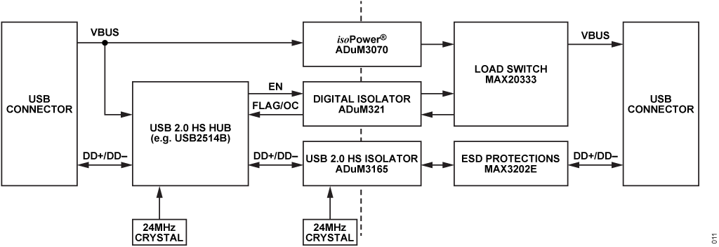
After the USB 2.0 high-speed hub is correctly set up, it enables power to the peripheral. If an overcurrent is flagged, the hub can stop power delivery to the USB downstream connector. The enable and overcurrent detection signals connected to the MAX20333 load switch can be isolated using the ADuM321 2-channel digital isolator. In CN0590, the differential pairs are isolated using the ADuM3165, while the isoPower is isolated through the ADuM3070 combined with an external transformer.
POWER DELIVERY WITH MAX77958
The MAX77958 is a highly customizable and robust solution for USB Type-C CC detection and power delivery protocol implementation. The block diagram shown in Figure 12 illustrates a possible implementation of an isolated power delivery host application, including USB 2.0 high speed signaling isolation.

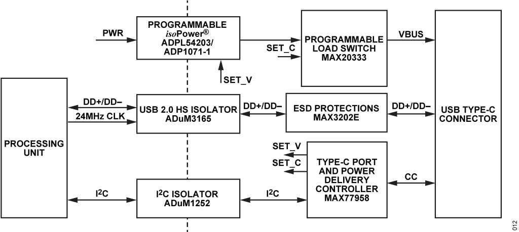
The isoPower circuity must be designed to meet the desired power capabilities, and this information must be stored in the registers of MAX77958 to be discoverable by the USB sink devices. A discrete isoPower design (for example, an ADP1071-1 based design using external power transistors) is required to support the full range of power of the PD standard (240W) and consequently all combinations of voltage and current values typical of power delivery devices. Use the ADPL54203 monolithic micropower isolated flyback converter to support PD up to 5V/3A (15W). The ADPL54203 operates from an input voltage range of 3.2V to 40V and delivers up to 17W of isolated output power integrating a 3.4A/60V power switch. This device is available in a compact thermally enhanced 8-lead SO package.
A typical power delivery connection sequence works as follows:
- The power roles are identified by the pull-up and pull-down resistors.
- The source capability written in the registers of MAX77958 are read by the sink through the CC channel.
- The sink requests one of the source voltage and current possibilities.
- The source accepts and the MAX77958 configures the output VBUS and maximum current to the desired or requested level.
ALTERNATIVE POWER OPTIONS
The ADuM4070 is an excellent replacement providing a C&C of 8mm in cases where 3.1mm C&C is not sufficient .This device features the same maximum power levels that ADuM3070 can achieve while offering more isolation protection.
The LT8302/LT8302-3 is an excellent solution when more than 2.5W of power is required. This device is a monolithic micropower isolated flyback converter. By sampling the isolated output voltage directly from the primary side flyback waveform, the part requires no third winding or digital isolator for regulation. The LT8302/ LT8302-3 operates from an input voltage range of 3V to 42V and delivers up to 18W of isolated output power. The Power Delivery with MAX77958 section discusses a solution for 15W of isolated output power using the ADPL54203.
Consider using the MAX13253 for intermediate power levels, for example for standard 900mA at 5V (USB 3.0 default power). This device is a 1A, push-pull, transformer driver designed to provide a simple solution for low EMI isolated power supplies. The MAX13253 operates from a single +3.0V to +5.5V supply, with up to 1A of continuous current and features integrated protection including fault detection, overcurrent protection, and thermal shutdown.
Circuit Evaluation & Test
The CN0590 was functionally tested with different USB 2.0 host and devices to verify its interoperability and transparency for a USB 2.0 connection successfully. For detailed instructions on the setup, refer to the CN0590 User Guide.
EQUIPMENT NEEDED
- EVAL-CN0590-EBZ evaluation board
- Host PC (must support high-speed USB 2.0)
- USB flash drive (must support high-speed USB 2.0)
- USB Type-C cable (must support both power and data signaling)
- Type-C male to Type-A female adapter
SETUP AND TEST
To test the USB 2.0 functionality of the EVAL-CN0590-EBZ, follow below steps.
- Using the Type-C to Type-A adapter, connect the USB flash drive to P6 of EVAL-CN0590-EBZ.
- Connect the USB Type-C cable to P1 of the EVAL-CN0590-
EBZ, and then the other end of the cable to the computer
USB port. Wait for the USB flash drive to be detected on the
computer.


Figure 13. CN0590 High Speed Data Transfer Test Setup - Validate the speed of the USB flash drive using a USB device tree viewer. Figure 14 shows an example device tree of a high-speed USB device.


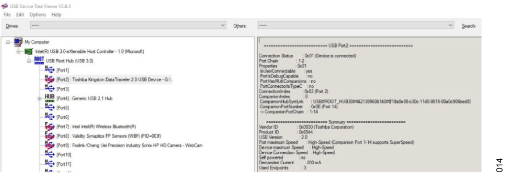
Figure 14. Example USB Device Tree Viewer Screen for a High-Speed USB Device

