CN0571
Galvanically Isolated Full HD 1080p/60Hz HDMI PHY Using iCoupler Isolation Technology


Overview
Design Resources
Design & Integration File
- Bill of Materials
- Layout
- Schematics
- Allegro Layout File
- Assembly Files
- Fabrication Files
-
Download Design Files
5.11 M
Features & Benefits
-
Circuit Evaluation Boards
- CN-0571 Circuit Evaluation Board (EVAL-CN0571-EBZ)
-
Design and Integration Files
- Schematics, Layout Files, Bill of Materials
Documentation & Resources
-
CN0571 User Guide1/16/2025WIKI
Circuit Function & Benefits
While galvanic isolation is typically not found implemented in a multimedia interface such as HDMI®, many applications require the presence of such an isolation barrier. In general, galvanic isolation enables an interface with immunity to noise, ground loops, and electrical line surges, while providing a safety barrier against electric shock for personnel and low voltage electronics. Certain applications, especially in the medical space, mandate this electrical safety via relevant safety certification bodies and standards.
Traditionally, the challenges associated with implementing a galvanically isolated gigabit digital interface, such as High-Definition Multimedia Interface (HDMI), have made it typically cost and time prohibitive, with solutions limited to optical fiber or complex serialization/deserialization (SERDES) circuits. Recent advances in high-speed digital isolation technology from Analog Devices, Inc., provides unique options to system designers wishing to isolate high resolution video interfaces.
Building on the previous CN-0422 design (720p resolution Isolated HDMI), this circuit note describes a complete solution for implementing an isolated HDMI port at up to 1080p resolution providing two means of patient protection (2MOPP) against secondary circuits, and one means of patient protection (1MOPP) against mains circuits for medical applications. The design is based on Analog Devices 2.5Gbps isolated low-voltage differential signaling (LVDS) transceivers (ADN4624) and includes the AD8195 HDMI buffer for compensating long cable losses.
Various applications require the addition of galvanic isolation to high-speed video interfaces or external video ports, some examples are discussed in this document.
Display Output for Patient Care
Patient care and vital signs monitoring equipment, such as ventilators and electrocardiograms (ECGs), feature a direct connection to a patient for breathing assistance and sensing. An integrated display within these monitoring units provides critical information regarding the patient. The displays located inside medical equipment are known, trusted, and certified for use in accordance with the IEC 60601 standard. The same cannot be guaranteed for any off the shelf external TVs and displays. This prohibits their use as long as the medical equipment is connected to the patient unless a means of protection (MOP) is provided between the external display and the patient.
The ability to connect clinical monitoring equipment to external displays offers certain advantages. These include extending the equipment display several meters away from the source, allowing remote monitoring of patients from outside of infectious wards, minimizing exposure to medical professionals. By removing the integrated display entirely, the device can be further miniaturized.
To ensure patient safety, any external connections from the medical equipment to peripheral devices, including display ports, must provide an isolation barrier for patient protection as shown in Figure 1.


Figure 1. Example of isolation barriers in a typical class I healthcare system.
The EVAL-CN0571-EBZ reference design provides a drop-in, plug and play solution for implementing an isolated HDMI display output port within a medical device, while meeting stringent medical safety standards such as IEC 60601.
Robust Human Machine Interface (HMI)
A human machine interface (HMI) is used in factory automation and process control to display programmable logic controller (PLC) data in a human readable format. With motors and pumps connected to the DIN rail mounted PLC, there is a possibility of indirect transient overvoltages on the HMI. In some instances, the HMI is located far away from the machine. Long cables create ground loops issues; therefore, increasing the impact of radiated noise on the signals. Isolation embedded in the video interface can prevent some of these issues from happening.
Isolation in the EVAL-CN0571-EBZ circuit increases system safety and robustness by providing protection against electrical line surges, breaking the ground connection between bus and digital pins, thereby removing dangerous ground loops within the harsh system.
HDMI 1080P Isolation Challenges and Benefits
The isolation of a video port presents unique challenges. The bandwidth requirements for standardized interfaces to displays vastly exceed what can be realized using a reasonable amount of optocouplers or standard digital isolators combined with SERDES circuits. Further complexity is added when attempting to isolate the entire signal chain of the video interface. For example, the HDMI protocol requires transition minimized differential signaling (TMDS) to carry Gbps video data and sideband signals to ensure video connection is established. This means that, in addition to power circuitry, there are further signals, all requiring isolation, which include the following:
- The display data channel (DDC), a bidirectional control signals to exchange video/format information.
- Consumer electronic control (CEC), a single-ended optional serial bus for the remote control of consumer devices.
- Hot plug detect (HPD), a single-ended active high signal to monitor the connection and disconnection state of display (sink) devices.
These signals must all be considered when adding galvanic isolation, and the resulting complexity often presents a barrier for system designers. Analog Devices provides a reference design for the galvanic isolation of the HDMI video protocol up to 1080p/60Hz resolution, which allows for drop-in safety protection in cases where patient/operator protection and noise robustness against common-mode transient immunity (CMTI) events and ground loops are desired or mandatory in the customer end application.
The system can transparently isolate an HDMI interface that is configured for resolutions of up to 1920p × 1080p (1080p) at 60Hz and is rated to a withstand voltage of 5000Vrms per UL 1577. The EVAL-CN0571-EBZ working voltage is limited by the ADuM4070 to a VIORM of 849Vpk per IEC 60747-17. The overall minimum system creepage and clearance (C&C) is 8mm. These characteristics make the EVAL-CN0571-EBZ reference design suitable for basic and reinforced IEC 61010/IEC 62368/IEC 60601 regulated applications.
The circuit shown in Figure 2 provides a completely galvanic isolated connection between an HDMI source and an HDMI sink device. Both signal and power isolation ensure a safe and noise immune connection between an HDMI source (for example, a processor) and an HDMI sink (for example, a display).


Figure 2. Simplified circuit diagram for EVAL-CN0571-EBZ.
Several versions of the HDMI standard are available. The circuit shown in Figure 2 is timing and voltage compatible to Version 1.3a of the HDMI standard. The circuit in Figure 2 includes isolation of high-speed TMDS clock and data lines, which are implemented with current-mode logic (CML) on the physical layer. It also provides the isolation of the consumer electronics control (CEC), hot plug detect (HPD), display data channel (DDC), and power signals. All the components used in EVAL-CN0571-EBZ passed the CISPR 32 Class B for easy integration in many protected environments.
Circuit Description
Figure 3 shows a simplified block diagram of the power isolation and the isolation of the HDMI signals. Section 1 through Section 5 details the various signals in the HDMI protocol and how each signal is isolated using the ADN4624, ADuM1252, ADuM4070, ADuM321N, and ADuM1252/ADN4622 devices as shown in Table 1.


Figure 3. Isolated 1080p HDMI signal chain diagram.
| Signals | Device | Section |
| Power | ADuM4070 | 1 |
| HPD | ADuM321N | 2 |
| DDC | ADuM1252 | 3 |
| TMDS | ADN4624 | 4 |
| CEC | ADuM1252/ADN4622 | 5 |
The design represents an isolated source application. In this scenario, long cables are expected to be driven and, therefore, the AD8195 HDMI 1.3a buffer from Analog Devices is used to enhance the cable driving capabilities of the isolator. In the Common Variations section, another version of the board is described, which does not make use of the buffer, more suitable for isolated sink or compact embedded applications where short printed circuit board (PCB) traces connections are driven by the ADN4624 Gbps isolator.
Step 1: Power
In the EVAL-CN0571-EBZ, an external supply must be connected to the Type C USB port to power all the ICs in the board. The minimum power that an HDMI source guarantees is limited by the HDMI standard to 275mW (5V at 0.055mA), not enough to power all the ICs in the EVAL-CN0571-EBZ. In a most common case scenario, and, therefore, in an isolated HDMI source application, where isolation is embedded in the board of the video transmitter (source), the power is not coming from an HDMI cable but from an on-board DC-DC or linear converter. Therefore, the power is not limited, and the accessory Type C USB connector can be removed by the design.
The Type C USB port provides the necessary 5V supply rail to power the board. The 3.3V and 1.8V voltage rails in the sourcefacing side of the barrier are generated by two ADP1707 linear dropout regulators. Sufficient power must also be provided to any circuitry located on the isolated side. To meet these requirements while maintaining galvanic isolation, the EVAL-CN0571-EBZ uses the ADuM4070, a 2.5W regulated DC-DC isolated power supply controller with an internal metal-oxide semiconductor field effect transistor (MOSFET) driver combined with an external push-pull transformer (see Figure 4).


Figure 4. Isolated power with ADuM4070 simplified block diagram.
The ADuM4070 based regulated push-pull converter in the EVALCN0571-EBZ utilizes two ferrite beads for filtering and suppression of electromagnetic interference (EMI) and common-mode noise.
Two RC snubbers are designed, tested, and optimized to minimize the oscillations resulting from the ringing of the transformer primary leakage inductance with the COSS of the MOSFET at turn-off, and the ringing of the transformer secondary leakage inductance with the rectifying diode reverse capacitance at turn-off, for an integration in an ideal low noise, low radiation environment.
The ADuM4070 can deliver the required current at up to a maximum ambient temperature of 105°C.
The isolated power coming from the regulated push-pull isolated converter configuration is provided to the HDMI sink on the DDC +5V line, the ADuM1252 I2C isolator used for DDC isolation, the ADuM321N digital isolator used for HPD and power enable isolation, and the two LTC3309A buck converters.
The first LTC3309A switching regulator is used to buck the 5V voltage down to 1.8V to power the ADN4624 VDD2 supply. The other LTC3309A is instead used to convert 5V down to 3.3V to power the optional ADuM1252 I2C isolator used for CEC isolation and the AD8195 buffer.
The choice of using a high-efficiency switching regulator on the secondary side of the barrier to buck the voltages to 3.3V and 1.8V comes from the limited 2.5W isolated power availability and to keep all components at a reasonable cool temperature during normal operation.
The +5V signal on the DDC line must only be provided to the HDMI sink when an HDMI source is connected. The +5V signal from an HDMI source is transmitted across the isolation barrier using one of the iCoupler® channels of the ADuM321N. This +5V signal is used in combination with a negative channel metal-oxide semiconductor (NMOS)-based inverter and a positive channel metal-oxide semiconductor (PMOS) to control the delivery of the +5V signal to the HDMI sink only when the above condition is met.
Step 2: Hot Plug Detect (HPD)
When an HDMI source device is connected to an HDMI sink device, the sink device receives a +5V signal, indicating that a source is connected. In response to this signal, the HDMI sink asserts the HPD signal, which is transmitted back to the source device. This indicates that the sink is correctly connected, and that it is ready to accept commands from the source through the DDC.
Figure 5 shows the HPD implementation on the EVAL-CN0571-EBZ reference design.


Figure 5. Hot plug detect and power isolation circuitry.
In the EVAL-CN0571-EBZ, the forward channel of the ADuM321N digital isolator is used to enable the 5V power to the output HDMI connector (facing the sink), only when an input HDMI cable is connected. In an isolated source application, the forward channel can instead be used as a power enable when the module or main processor goes into sleep mode.
The backward channel of the ADuM321N digital isolator is used to transmit the HPD signal across the isolation barrier from the sink to the source. A 4.7kΩ pull-down resistor on the input prevents the HPD signal from asserting when a sink device is not connected. A 1kΩ series resistor on the output is used to meet the 1kΩ ±20% output resistance specification for the HPD signal in the HDMI standard. This 1kΩ series resistor is not necessary in embedded applications. A 4.7kΩ pull-down resistor on the output prevents the HPD signal from asserting if a source is connected before the EVAL-CN0571-EBZ circuitry is powered correctly.
To enable the power flow to the sink, a discrete load switch is designed with an NMOS and a PMOS transistor. The NMOS serves as an inverter while the PMOS as the actual load switch. Analog Devices offers a variety of load switch ICs in its portfolio. An example is the MAX891, which can also act as a programmable current limiter, offering a rugged overcurrent protection.
Step 3: Display Data Channel (DDC)
The DDC is used for configuration and status exchange between the source and sink. The HDMI source device uses the DDC to read the extended display identification data (EDID) from the sink device. The EDID contents determine what audio/video formats are possible at the HDMI sink. The DDC channel is also used in the implementation of High-bandwidth Digital Content Protection (HDCP). The bidirectional DDC follows the requirements of a standard mode I2C bus, operating at a clock rate of 100kHz.
The DDC channel is isolated in the EVAL-CN0571-EBZ using the ADuM1252 bidirectional I2C isolator as shown in Figure 6. The serial clock (SCL) line requires a source pull-up of 47kΩ and a sink pull-up of 1.8kΩ. The serial data (SDA) line requires a sink pull-up of 1.8kΩ, with no source pull-up (since integrated in every HDMI compliant source).


Figure 6. DDC isolation with ADuM1252 and AD8195.
Step 4: Transition Minimized Differential Signaling (TMDS)
The video and audio data in HDMI are transmitted from source to sink using four lanes of TMDS. The TMDS signals consist of three data pairs and one clock pair: TMDS_DATA0±, TMDS_DATA1±, TMDS_DATA2±, and TMDS_CLK±. The three differential data pairs transmit 10 bits per clock period and carry the high-speed video and audio data. The TMDS clock and data lines are implemented with the CML physical layer.
The coupling networks shown in Figure 7 allow reliable translation between CML and LVDS voltage levels. Following the coupling between the CML and the low-voltage differential signal (LVDS) physical layer, the ADN4624 2.5Gbps LVDS isolator is used to isolate the TMDS signals.


Figure 7. TMDS isolation circuitry and voltage levels.
For CML to LVDS coupling, use 50Ω pull-up resistors to correctly terminate the CML pairs to the 3.3V supply. Series AC-coupling capacitors are required to remove the CML DC common-mode voltage (3.1V) that is not compatible with the absolute maximum voltage of the input data pin of the LVDS isolator. The EVAL-CN0571EBZ circuit note uses 10nF capacitor AC coupling capacitor for the purpose. A resistor divider per each line made of a 10kΩ pull-up resistor to 1.8V and a 13kΩ pull-down resistor to ground biases the common mode of the LVDS signals to 1V, which is the optimum point minimizing the resulting deterministic jitter. Two series 62Ω damping resistors are used, between the AC-coupling capacitors and the common-mode bias network, to reduce reflections caused by the capacitive input of the isolator. In the case of isolated source applications, the optimum coupling network must follow the design guidelines of the processor itself. Sometimes, video transmitters can be either configured both for DisplayPort and HDMI protocols and, therefore, their output is always AC-coupled, even though the standard TMDS are DC-coupled and do not require any AC coupling. In that case, the optimum CML to LVDS network would be a T-termination to 1V.
For LVDS to CML coupling, use a minimum of 10nF capacitors to remove the DC common-mode voltage of the ADN4624 LVDS outputs. A high capacitance value for the AC coupling capacitor has a better long-term DC wander effect and series impedance, but a worse equivalent series resistance (ESR) and, therefore, a resonance point at lower frequencies. A good compromise, for the LVDS to CML coupling network is a value in between 10nF to 100nF. The CML inputs at the HDMI sink are terminated with 50Ω on each line to the supply rail of the sink. This supply referenced termination removes the need of biasing resistors in the LVDS to CML coupling block.
The ADN4624 does not include any equalization or preemphasis capabilities to drive long cables and recover from resulting channel insertion losses. To enhance the capabilities of the isolator and recover the intersymbol interferences (ISI) jitter, an HDMI repeater or signal conditioner can be used. The EVAL-CN0571-EBZ makes use of the AD8195 HDMI buffer for this purpose. For maximum cable length driving capabilities, refer to the AD8195 data sheet.
Step 5: Consumer Electronics Control (CEC)
The CEC signal is optional. It is a protocol that allows the high control functions of all connected audiovisual products (for example, remote control of a television to set up a DVD player) to be accessed by any device in the user environment. The physical layer of the CEC protocol is a bidirectional multipoint 3.3V single-ended bus with up to a maximum of 10 devices. The minimum bit period on the CEC bus is 400µs. The HDMI specification specifies a pull-up of 27kΩ for the CEC line.
As shown in Figure 8, the SDA bidirectional channel of the 3.3V powered ADuM1252 isolator is used to provide isolation of the CEC signal. The SCL channel is not used and is tied by means of a 2kΩ pull-up resistor to the supply rail. Each side needs to be connected to a pull-up resistor of 27kΩ. The CEC standard specifies a maximum off state leakage current of 1.8µA. To ensure that, a series Schottky diode is used on the primary side to limit the off state leakage current while the EVAL-CN0571-EBZ is unpowered. The secondary side 27kΩ resistor is integrated in the AD8195 HDMI buffer, thereby the ADuM1252 is connected straight to it without requiring any external pull-up.


Figure 8. CEC isolation circuitry with ADuM1252 isolator and AD8195 HDMI buffer.
The CEC channel can be implemented using a multiple channel isolator such as the ADuM6422A. The implementation of this solution is shown in Figure 9. This can be useful when compact applications are desired and bill of materials (BOM) minimization is important. The digital isolator outputs are push-pull and not suitable for bidirectional multipoint communication. A series of Schottky diodes and pull-up resistors are used to convert these to open-drain outputs. The reverse bias Schottky diodes allow the CEC line to be pulled low by the ADuM6422A VOB and VOC outputs (as shown in Figure 6), while remaining high-impedance during a logic high. The low 0.12V forward voltage drop of the BAT60 Schottky diode minimizes the impact on the noise margin during a logic low.


Figure 9. Consumer electronics control (CEC) isolation circuitry.
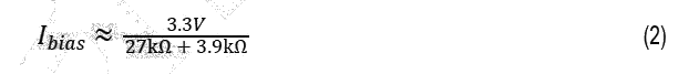
On the HDMI source side, to prevent the circuit from latching, a bipolar junction transistor (BJT) Q1 is used. This is polarized by the resistor divider and the Schottky diode (R2, R3, D1) slightly above its maximum base emitter voltage (VBE) threshold. The conduction status of Q1 depends then on its emitter voltage. When the VOC output is driven low by the sink facing side, the VOL is increased by an offset because of the forward voltage of the Schottky diode (D2) and the drop on the 3.9kΩ resistor. The resistor is sized as such to generate a low-voltage VVOL2, during backward communication, which keeps Q2 off and prevents latching to happen. The value of the CEC logic low during backward communication can be computed as follows:
VOL2(CEC) = VF(Ibias) + IbiasR5 + VOL(Ibias) ≈ 0.6 V
where Ibias can be approximated as,
The BAS40 Schottky diodes are used for temperature compensation and to limit off state leakage current while the circuitry is unpowered.
Summarizing, we can distinguish two modes of operation as follows:
- During forward communication, it is the source side driving the CEC line, and the communication directionality is from the source to the sink. If the source CEC is asserted, a low-logic value turns the BJT on and Logic 0 is transmitted to the other side of the barrier, thanks to the digital isolator top channel. When the source CEC is released, the output cannot go immediately to high level because of the remaining low-level signal caused by the bottom channel transmitting backward Logic 0. Therefore, it raises to VBE of Q1, Q1 goes in high impedance and then it is released.
- During backward communication, it is the sink driving the CEC line, and the communication directionality is from the sink to the source. If the sink CEC is asserted, the offset generated by D2 and the series resistor R5 keeps Q1, biased just above its threshold, off and prevents the circuit from latching. If the sink CEC is released, D2 is reverse biased, and the CEC line can raise to 3.3V, thanks to its 27kΩ pull-up resistor.
The CEC circuit in the image forms a discrete I2C/bidirectional isolator with two unidirectional channels (one backward and one forward) of a digital isolator. The values of the resistors and the behavior of the circuit were simulated with LTspice and the circuit functionality is verified in laboratory at room temperature
Layout Guidelines
When dealing with high-speed isolation, the layout becomes part of the solution and has a significant impact on the performance of the circuit. The layout of the EVAL-CN0571-EBZ reference design is optimized for superior signal integrity. The following is a subset of the most important layout guidelines to consider when designing a circuit for the isolation of HDMI 1080p/60Hz.
- Differential traces that carry the TMDS signals must be designed with a controlled differential impedance of 100 ± 15% ohms.
- If microstrip traces are used, there must be a continuous reference plane on the PCB layer directly below the traces.
- If stripline traces are used, they must be sandwiched between two continuous reference planes in the PCB stackup.
- Interlayer vias introduce impedance discontinuities that can cause reflections and the worsening of the jitter on the signal path. Therefore, it is preferable to route the TMDS lines exclusively on one layer of the board. If vias are unavoidable, place multiple via ground return paths very close to minimize the impedance discontinuity.
- To prevent unwanted signal coupling and interference, route the TMDS signals away from other signals and noise sources on the PCB.
- Both traces of the same differential pair must be equal in length to minimize intrapair skew. Excessive intrapair skew can introduce jitter through duty cycle distortion (DCD).
- Any group of four TMDS channels (input or output) must have closely matched trace lengths to minimize interpair skew. Severe interpair skew can cause the data on the four different channels of a group to arrive out of alignment with one another. A good practice is to match the trace lengths for a given group of four channels to within 0.05 inches on the FR4 material.
- The length of the TMDS traces must be minimized to reduce overall signal degradation. Commonly used PCB material, such as FR4, is lossy at high frequencies; therefore, long traces on the circuit board increase signal attenuation, resulting in decreased signal swing and increased jitter through ISI.
- Keep the CML to LVDS conversion network as close as possible to the isolator to minimize the length of the unwanted parasitic stub in-between. Use 0201 components and place the outer coupling networks 45 degrees angled to keep all the stubs at the same trace length.
- Use guard traces or ground planes between the TMDS pairs. This is to minimize crosstalk, electromagnetic radiation, and unwanted signal coupling or interference.
Common Variations
Isolated Sink Applications Topologies and Related Power Requirements
The EVAL-CN0571-EBZ is designed as an isolated repeater, where the isolation circuitry is integrated into an HDMI source. Some system design changes are required in the case the isolation is embedded in the sink side (display side). In that case, the following two options can be considered depending on where to use the AD8195 HDMI buffer in the signal chain:
- If the HDMI sink makes use of long input cables, it is desirable to use the AD8195 HDMI buffer at the primary side, namely at the input of the isolator rather than at the output. The reason is to better exploit the input equalization effect of the redriver, namely to recover and compensate the losses over the frequencies of long cables. In this case, the power requirements of the primary side of the isolated system remain practically unchanged with respect to the isolated source scenario described in the sections above. The ADuM4070, combined with an external transformer, is an excellent solution to deliver the necessary power.
- If the HDMI sink makes use of short input cables or short input traces, the HDMI buffer can be used at the secondary side of the isolation barrier, namely at the isolator output or dropped completely. In this case, the primary side power requirements decrease considerably with respect to an isolated source, and a more compact power isolation solution can be considered. For example, the ADuM4070 can be replaced with the ADuM6028/ ADuM6020 for the isolation of the 5V rail. These are fully integrated isolated DC-DC converters, which eliminate the need to design and build discrete converters in applications up to 500mW. This has the tangible effect of shrinking the HDMI isolated solution area. If the CEC must be isolated as well, the ADuM6422A solution described in the Step 5: Consumer Electronics Control (CEC) section helps to keep small form factors.
Alternative Nonisolated Power Circuitry
The ADN4624 2.5Gbps digital isolator leverages 1.8V power supply rails for reduced power consumption and precision timing performance. The EVAL-CN0571-EBZ circuit note uses two LTC3309As on the sink facing side of the barrier. These can be replaced with LTC3307A rated up to 3A.
On the source facing side of the barrier, two ADP7103s low noise linear regulator can be used to generate the 3.3V and 1.8V supply rails, in place of the two ADP1707, being rated up to 200mA. The 3.3V power supply rail is needed for supporting the CEC channel and the HDMI buffer.
Input HDMI Signal Conditioning
The HDMI specification references a receiver equalization block on a display sink to boost performance over long cable distances. The ADN4624 does not include receiver equalization capabilities. In isolated sink applications where full input compliance to the HDMI specification is desired, use the AD8195 HDMI buffer or signal conditioner to equalize signals received from the source. Place the buffer between the source facing connector and the CML to LVDS coupling network. In this case, the isolated power budget is increased by the HDMI buffer and is provided by the ADuM4070 as it happens for isolated HDMI source applications.Optional Utility Signal
The HDMI Ethernet and audio return channel (HEAC) is an optional channel. It was added in more recent versions of the HDMI standard (more recent than HDMI 1.3a).
It is a utility line that provides Ethernet-compatible data networking between connected devices and an audio return channel in the opposite direction of TMDS.
The circuit described in Figure 2 and Figure 3 do not include the isolation of the optional HEAC signaling.
Lower Creepage and Clearance and Isolation Rating Version
The digital isolators used in the EVAL-CN0571-EBZ reference circuit are rated to 5000Vrms per UL 1577 and feature a minimum of 8mm of creepage and clearance across the isolation barrier. These are suitable for basic and reinforced safety applications. For medical applications, the devices used in this design meet the withstand voltage and creepage requirements for 1MOPP, 1 means of operator protection (MOOP) against 250Vrms mains circuits, and 2 means of patient and operator protection against secondary circuits voltages (up to 50Vrms). In the case of functional isolation (introduced to guarantee system functionality) or basic isolation is needed, Table 2 helps the system designer choosing the proper isolators. Table 2 shows replacements for the isolators in the EVAL-CN0571-EBZ with a lower creepage and clearance version to allow more compact applications.
| Isolators Type | Functional Isolation Applications | Safety Isolation Applications | Safety Isolation Applications |
| Isolation Voltage | Up to 1.5kVrms | Up to 3kVrms | Up to 5Kvrms |
| Minimum Creepage | 1.27mm | 4mm | 8mm |
| DC-DC (Source Applications) | LT8301 | ADuM3070 | ADuM4070 |
| I2C Isolators | ADuM1252ARZ | ADuM1252ASA | ADuM1242AWA |
| Gbps Isolator | ADN4624BCPZ | ADN4620BRSZ | ADN4624BRNZ |
| Digital Isolator (Source Applications) | ADuM321N0BRZ | ADuM120N | ADuM321NzBRIZ |
Circuit Evaluation & Test
Power Sequencing
The EVAL-CN0571-EBZ requires to be powered by means of the Type C USB port with an appropriate power supply delivering a minimum of 5W. The EVAL-CN0571-EBZ must be powered and an LED must light up before connecting any sink or source to it. This ensures the correct operation and transparency of the isolation.
Common-Mode Transient Immunity (CMTI)
CMTI refers to the ability of an isolator to reject fast common-mode transients. CMTI is defined as the maximum common-mode voltage slew rate, or transient that can be tolerated between system ground (Ground 1) and isolated ground (Ground 2) while still maintaining bit error free communication.
CMTI is important because high slew rate transients can couple across the parasitic capacitance of the isolation barrier, corrupting data. The ADuM1252, ADuM321N, and ADN4624 are robust digital isolators with good CMTI performance, specified to operate correctly and without data corruption in the presence of typical common-mode transients of 100,000V/µs.
Radiated Emissions
Most of the systems require electromagnetic compliance testing before being integrated in any environment. This guarantees that the system does not alter the functionality of nearby circuits and is not being altered by the operation of nearby circuits, which can be both potential victims or aggressors, respectively.
Each of the digital isolators used in the EVAL-CN0571-EBZ passed the Class B CISPR 32.
HDMI Source Compatibility Testing
This section describes a HDMI source compatibility test performed with the EVAL-CN0571-EBZ. Five consecutive compatibility tests were passed using the EVAL-CN0571-EBZ outputs, including clock jitter, eye diagrams and jitter for data channels, rise and fall times for clock and data channels, and maximum/minimum clock duty cycles. Figure 10 documents the summary test results, while Figure 11 shows the configuration details.


Figure 10. HDMI source compatibility test summary.


Figure 11. HDMI source compatibility test configuration.
Figure 12 to Figure 14 show the HDMI source eye diagram tests for 1920p × 1080p, 60Hz HDMI resolutions for the three data channels.


Figure 12. HDMI source compatibility test eye diagram, 1080p, data channel 0.


Figure 13. HDMI source compatibility test eye diagram, 1080p, data channel 1.


Figure 14. HDMI source compatibility test eye diagram, 1080p, data channel 2.
System Compatibility Test
The Analog Devices EVAL-CN0571-EBZ was tested with multiple HDMI sources and sinks to verify its system compatibility and transparency for an HDMI 1080p/60Hz video link.
The following is a list of devices that has been tested in combination with the EVAL-CN0571-EBZ and different monitors:
- NVIDIA® Jetson Nano
- Dell® PCs
- Dell® Docking Stations
- UGREEN® Hub
Learn More
CN-0571 Design Support Package
High-Definition Multimedia Interface (HDMI). www.hdmi.org.
Data Sheets and Evaluation Boards
EVAL-CN0571-EBZ Evaluation Board
EVAL-ADN4624EB1Z Evaluation Board
I2C refers to a communications protocol originally developed by Philips Semiconductors (now NXP Semiconductors).