CN0432


Overview
Design Resources
Design & Integration File
- Schematic
- Bill of Materials
- Gerber Files
- Allegro Files
- Assembly Drawing
Evaluation Hardware
Part Numbers with "Z" indicate RoHS Compliance. Boards checked are needed to evaluate this circuit.
- AD9139-DUAL-EBZ ($582.62) Dual Synchronized AD9139 Board
- AD-DPG3 Digital Pattern Generator Platform
Device Drivers
Software such as C code and/or FPGA code, used to communicate with component's digital interface.
Features & Benefits
- Wide IQ Bandwidth (1150 MHz)
- Low Error Vector Magnitude (EVM)
- Synchronous Channels
Product Categories
Markets and Technologies
Parts Used
Documentation & Resources
-
CN0432 User Guide9/19/2019WIKI
Circuit Function & Benefits
This circuit shown in Figure 1 provides a synchronized, wideband transmitter, which can support a very wide I/Q bandwidth of up to 1150 MHz. The design proves high in-band signal performance such as high spurious-free dynamic range (SFDR), low error vector magnitude (EVM), and flat frequency response over a wide band.
The synchronization performance between multiple channels is especially critical for the quadrantal error correction (QEC). The delay mismatch between the converters can be within one clock cycle when multichip synchronization is enabled, and a well-aligned sync clock is present.
The challenge of high speed synchronization is to reach the accuracy of digital-to-analog (DAC) clock cycles over process, voltage, and temperature (PVT). To achieve that accuracy, a synchronization logic block is implemented on the DAC, and a careful layout and clock scheme on board must be designed to work with the synchronization logic block.
This circuit can be used to support wideband point-to-point applications in E-band, which ensures both zero intermediate frequency (ZIF) and complex intermediate frequency (CIF). The excellent synchronization performance makes it possible to support the strict alignment requirements found in applications like radar.


Circuit Description
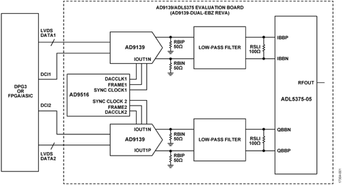
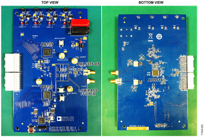
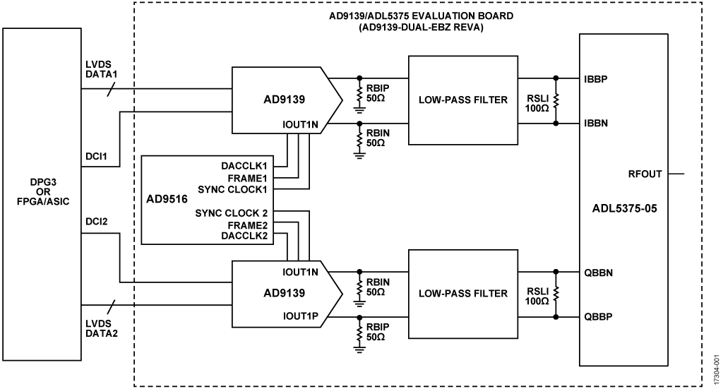
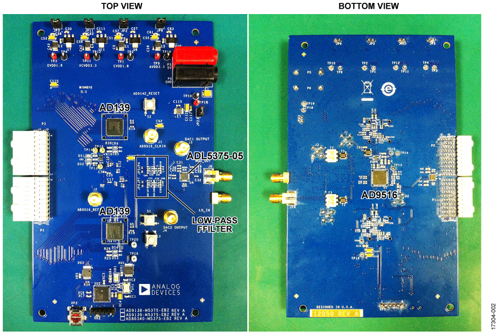
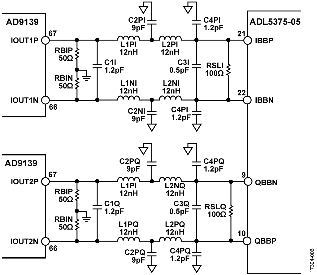
The board shown in Figure 2 uses the dual AD9139 single-channel TxDAC, the ADL5375-05 wideband quadrature modulator, and the AD9516-1 clock generator.
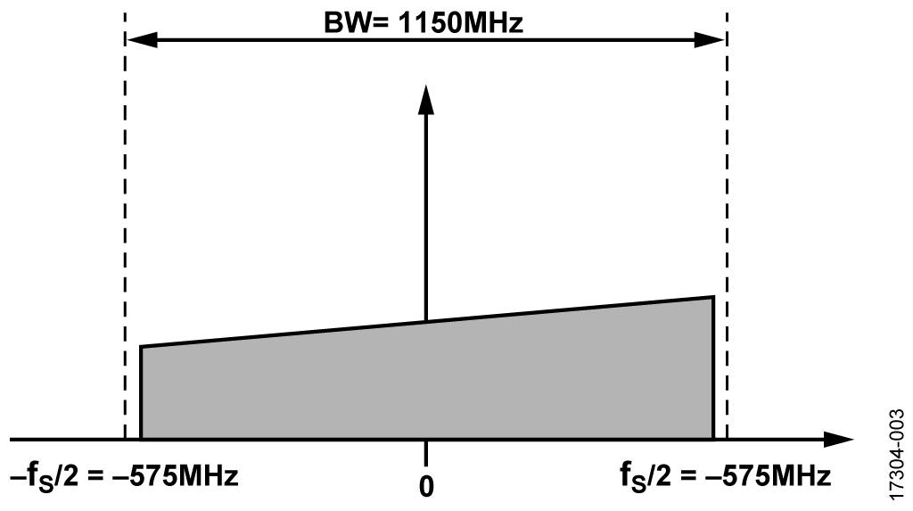
The maximum data clock input (DCI) frequency of the AD9139 can be up to 575 MHz. Because the data captured at both rising edge and falling edge feeds to one single DAC, the maximum data rate at 1× mode can reach as high as 1150 MSPS. To support quadrature data, two AD9139 devices are used to generate baseband data. The analog output of every channel goes to its own low-pass filter, respectively. Therefore, the reference design can support a maximum complex bandwidth of up to 1150 MHz, as shown in Figure 3. The flatness over such a wide range is critical. Because the AD9139 includes an inverse sinc filter that cancels the effect of the DAC’s inherent sinc roll off, the flatness of the filter after DAC becomes important to the total flatness. A DDR clock frequency of 575 MHz is very high for a parallel low voltage differential signals (LVDS) interface. The timing of the LVDS interface needs to be designed carefully.

Quadrature Modulator
The ADL5375-05 is a broadband quadrature modulator with an output frequency range of 400 MHz to 6 GHz. The ADL5375-05 interfaces with the AD9139 as the I/Q modulator, which covers a wide frequency range from 400 MHz to 6 GHz. The output of the AD9139 and the input of the ADL5375-05 share the same common mode level of 0.5 V.
Clock Generation and Considerations
Considering the synchronization requirements, the DACCLK, sync clock, and frame clock of both AD9139 devices must be well aligned. The AD9516-1 supports the necessary clock distribution functions, as well as a voltage controlled oscillator (VCO) and phase-locked loop (PLL) integrated for higher frequency generation. With the VCO and PLL disabled and the AD9516-1 in clock distribution mode, the phase noise of the clocks is better for the high speed alignment. In clock distribution mode, the additive phase noise at 10 MHz offset with divider = 1 and 1 GHz output is −147 dBc/Hz. The Rohde & Schwartz SMA100A has excellent phase noise performance; used as the input of the AD9516-1, the total phase noise at the AD9516-1 output is close to the limit of the minimum value of the AD9516-1 in clock distribution mode.
Multichip Synchronization of AD9139
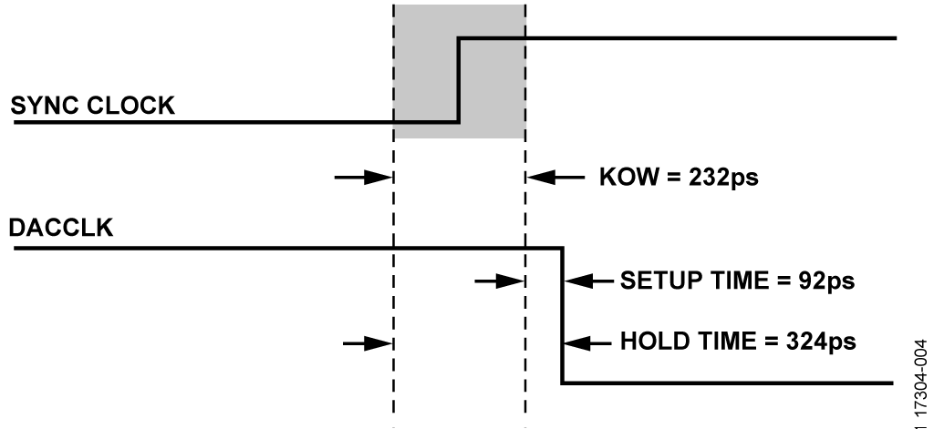
The synchronization between dual channels is critical to QEC. Layout symmetry between DACCLK and sync clock is required. In addition, the phase between DACCLK and sync clock must not fall in the setup and hold time window (also called the keep out window (KOW)).
The mechanism of synchronization can reach the performance of less than one DAC clock cycle mismatch between multiple channels over PVT on the DAC output. The following are guidelines to achieve the test performance:
- DACCLK 1 and DACCLK 2 must be well aligned on the pins of the AD9139. Mismatch between DACCLK 1 and DACCLK 2 is added to the final mismatch on the output.
- Sync Clock 1 and Sync Clock 2 must be well aligned, and they are sampled by DACCLK1 and DACCLK2, respectively, and used as the reference.
- The relative phase between DACCLK and sync clock must not fall in the KOW, as shown in Figure 4.

LVDS Interface Design
When DCI = 575 MHz, it is usually a challenge for LVDS interface design over PVT. This section shows how to design and optimize the interface through one example.
In Figure 5, as an example, DCI = 491 MHz. If the edge of DCI and DATA are well aligned on the pin of the AD9139, based on the AD9139 data sheet specifications, the KOW (setup time + hold time) can be placed in the middle of the valid window when the delay locked loop (DLL) phase is set to zero.

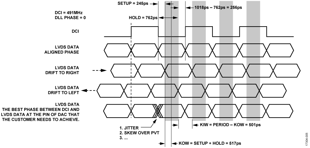
The data valid margin is defined by the following equation.

Over process variation, voltage, and temperature, TDATA VALID MARGIN must be > 0 to make sure that the data is sampled correctly.
When DCI = 491 MHz (see Figure 5),
- TDATA PERIOD = 1018 ps
- THOLD + TSETUP = 517 ps
- TDATA SKEW + TDATA JITTER must be less than 501 ps over PVT, which is the requirement for the user’s implementation. TDATA SKEW includes LVDS data bus delay mismatch, the skew between DCI and DATA bus over PVT, and so on.
To optimize the interface design, the user can do the following:
- Route the tracks with equal length and as short as possible on the printed circuit board (PCB).
- Optimize the programmable field gate array (PFGA) by ensuring the following:
- The edges of DCI and DATA are well aligned on the pins of the AD9139.
- The drift between DCI and DATA is as small as possible over temperature and voltage.
- The jitter of DCI and DATA is as small as possible.
With the DLL phase swept, the sample error detection (SED) function of the AD9139 can also be used to check the timing relationship between DCI and DATA.
Low-Pass Filter Design
For experimental purposes, in order not to limit the performance of AD9139 due to the filter, a filter with good flatness and group delay performance within 240 MHz was designed on the board. The out-of-band rejection can be enhanced by increasing the order of the filter in real product development.
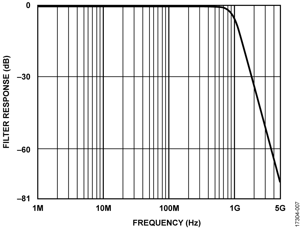
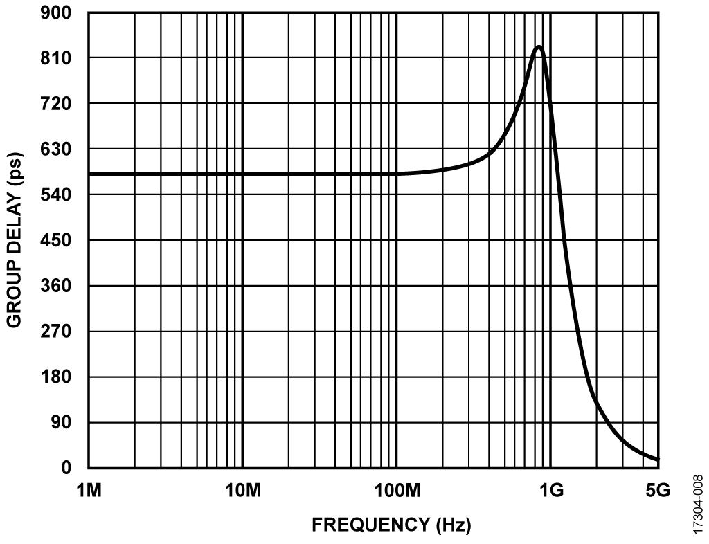
The filter topology shown in Figure 6 is a fifth-order Butterworth filter with a 900 MHz corner frequency. The simulated response of the filter is shown in Figure 7. The simulated flatness is ±0.1 dB from dc to 240 MHz. The simulated group delay of the filter is shown in Figure 7.


Layout Recommendations
Special care must be taken in the layout of the AD9139 and ADL5375 interface. The following are some recommendations for good noise and spurious performance. Figure 9 shows a top-level layout, which follows these recommendations:
- Place the DAC, filter, and modulator on the same side of the PCB.
- Tightened filter layout: cut down the keep out margin of L and C.
- Triple ground the shunt caps to the GND plane.
- Shorten the distance from DAC to the modulator.
- Keep all I/Q differential trace lengths well matched.
- Place the filter termination resistor as close as possible to the modulator input.
- Place the DAC output 50 Ω resistors as close as possible to the DAC.
- Use 0402 size for L and C.
- Thicken the trace widths through the filter network to reduce signal loss.
- Place vias around all the DAC output traces, filter networks, modulator output traces, and LO input traces.
- Route the local oscillator (LO) and modulator outputs on different layers or at 90° angle to each other to prevent coupling.

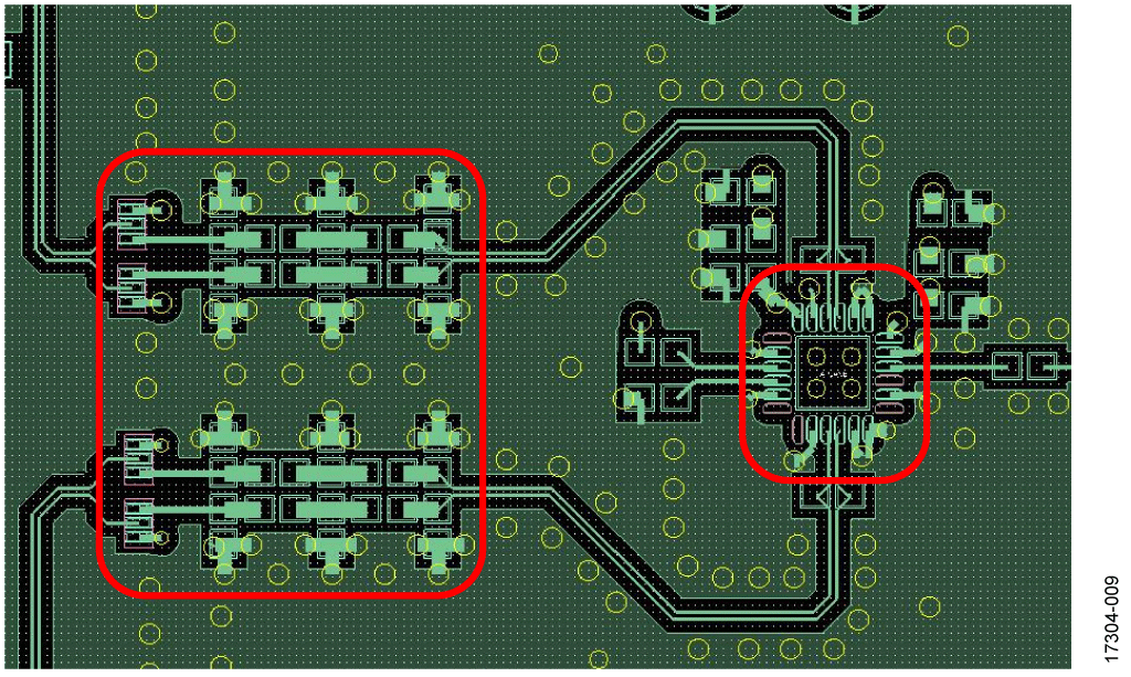
Further information on proper layout can be found in the AD9139-DUAL-EBZ layout files included in the design support package at www.analog.com/CN0432-DesignSupport.
Circuit Evaluation & Test
The following section describes how to set up and test the board. These steps outline the basic steps required to replicate the demo and results. For more detailed information, see the AD9139-DUAL-EBZ Evaluation Board Quick Start Guide.
Required Equipment
The following hardware is required:
- AD9139-DUAL-EBZ
- AD-DPG3
- Agilent E3631A power supply (or equivalent)
- Spectrum Analyzer PXA N9030A
- Rohde & Schwartz SMA100A signal generator
- PC with USB port
- USB cable
The following software is required:
- DPG downloader
- ACE software
Test Setup
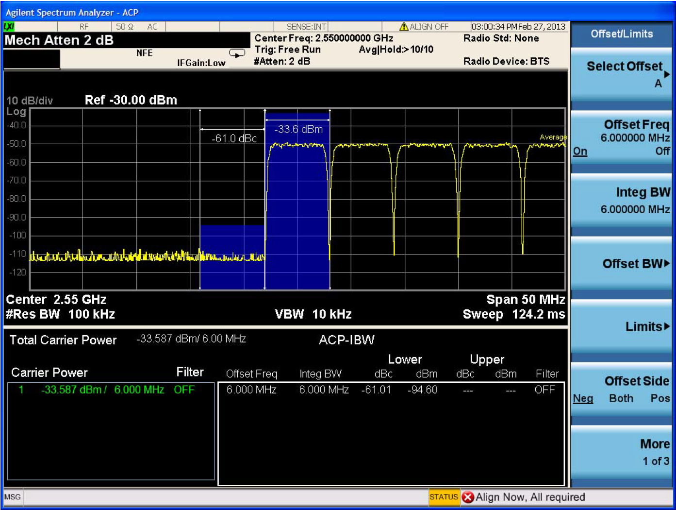
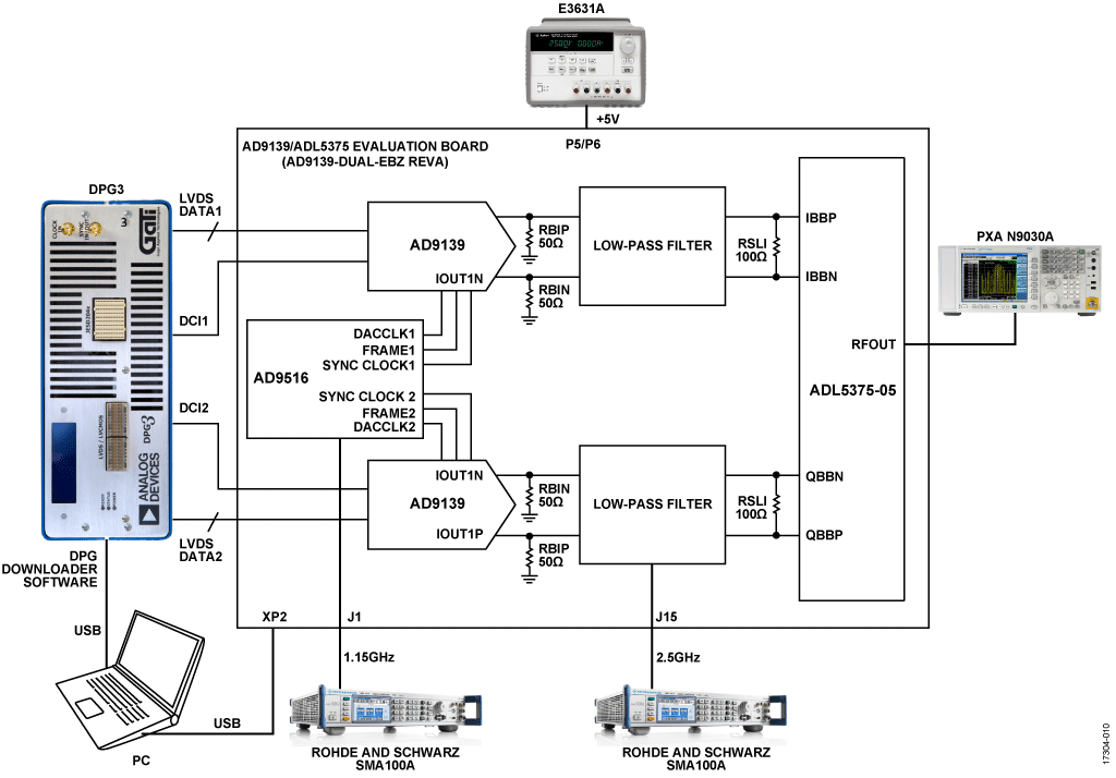
The following section describes details of measuring adjacent channel power (ACP) and modulation error ratio (MER) performance with the digital modulation of 64 QAM. The test setup is flexible and allows other measurements to be performed. The test setup is shown as below in Figure 10. The hardware of the AD9139-DUAL-EBZ evaluation board,
SPI software, quick start guide (QSG), and DPG3 hardware and software are all released.
One Keysight E3631 is used to provide the 5 V power supply of the board on P5/P6. One R&S SMA100A provides the input clock to the AD9516-1 on the board. A second R&S SMA100A provides the LO clock to ADL5375-05. The AD9139 is programmed by serial peripheral interface (SPI) software. The vector transmitted by the AD9139 is generated and downloaded to the DPG3 by DPGDownloader, which runs on the PC. The output of the ADL5375-05 feeds to the Keysight PXA N9030A.

Measured Results