CN0232


Overview
Design Resources
Design & Integration File
- Schematic
- Bill of Materials
- Gerber Files
- PADS Files
- Assembly Drawing
Device Drivers
Software such as C code and/or FPGA code, used to communicate with component's digital interface.
ADF4350 GitHub Linux Driver Source Code
ADF4153 GitHub no-OS Driver Source Code
ADF4350 GitHub no-OS Driver Source Code
ADF4153 FMC-SDP Interposer & Evaluation Board / Xilinx KC705 Reference Design (Wiki Link)
Features & Benefits
- Generate frequencies from 137.5 MHz to 4400 MHz
- Increased frequency resolution
Product Categories
Markets and Technologies
Parts Used
Documentation & Resources
-
UG-167: Evaluation Board for the ADF4153 Fractional-N PLL Frequency Synthesizer9/14/2015PDF250 kB
-
UG-110: Evaluation User Guide for ADF43503/16/2010PDF403 kB
-
Fundamentals of Phase Locked Loops (PLLs)2/14/2015PDF407 kB
-
MT-101: Decoupling Techniques2/14/2015PDF954 kB
-
MT-031: Grounding Data Converters and Solving the Mystery of "AGND" and "DGND"3/20/2009PDF144 kB
Circuit Function & Benefits
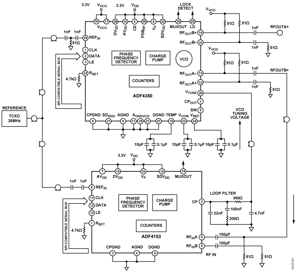
The circuit shown in Figure 1 uses the ADF4350 synthesizer with an integrated VCO and an external PLL to minimize spurious outputs by isolating the PLL synthesizer circuitry from the VCO circuit.
Devices with integrated PLLs and VCOs may have feed through from the digital PLL circuitry to the VCO, leading to higher spurious levels due to the close proximity of the PLL circuitry to the VCO.
The circuit shown in Figure 1 uses the ADF4350, a fully integrated fractional-N PLL and VCO that can generate frequencies from 137.5 MHz to 4400 MHz, together with the ADF4153 PLL.
In addition to improvements in spurious performance, another possible advantage of using an external PLL is the possibility of increased frequency resolution. For example, if the ADF4157 PLL is selected in place of the ADF4153, the frequency resolution of the PLL can be as fine as 0.7 Hz.

Circuit Description
The ADF4350 is a wideband PLL and VCO consisting of three separate multiband VCOs. Each VCO covers a range of approximately 700 MHz (with some overlap between the frequencies of the VCO). This permits a fundamental VCO frequency range of between 2.2 GHz to 4.4 GHz. Frequencies lower than 2.2 GHz can be generated using internal dividers within the ADF4350.
For most applications, the internal PLL of the ADF4350 is used to lock the VCO. In addition to locking the PLL, the PLL circuitry performs an additional vital function of VCO band select, using the internal reference (R) and feedback (N) counters of the internal PLL to compare the VCO output with the reference input. For frequency generation, the internal PLL must be enabled and the desired frequency must be programmed. Then, once sufficient time has elapsed for band select, the internal PLL can be disabled, and, finally, the external PLL can be enabled. The external PLL compares the reference frequency and the VCO output frequency to generate a stable dc voltage to lock the PLL.
Figure 2 shows the output frequency spurs measured at RFOUTA+ using the ADF4350 internal PLL and VCO with the ADF4153 PLL disabled. Note the presence of PFD spurs at 13 MHz and 26 MHz.
Figure 3 shows the output spurs measured at RFOUTA+ with the ADF4350 internal PLL circuit disabled and the external ADF4153 PLL active. In this mode, the charge pump output of the ADF4153 drives the loop filter, which in turn drives the VTUNE input of the ADF4350. The VTUNE input controls the ADF4350 VCO output frequency.
In making a comparison between Figure 2 and Figure 3, the spurs due to the phase frequency detector (PFD) frequency, at 13 MHz and 26 MHz, in Figure 2 have disappeared into the noise floor in Figure 3.
Common Variations
Different PLLs can be selected. The fractional-N PLL in both the ADF4350 and ADF4153 has a minimum frequency resolution of PFD/4095. If finer resolution is required, the ADF4157 can be selected. The resolution of this PLL is PFD/225, thereby providing an ultrafine resolution of <1 Hz.
For applications requiring simpler software programmability, the ADF4150 PLL is software compatible with the ADF4350, easing the software programming sequence.


Circuit Evaluation & Test
The CN-0232 uses the EVAL-ADF4350EB2Z board for evaluation of the described circuit, and with some minor modifications, allows for quick setup and evaluation. The EVAL-ADF4350EB2Z board uses the standard ADF4350 programming software, contained on the CD that accompanies the evaluation board. The EVAL-ADF4153EBZ1 evaluation board comes with the software for the ADF4153 PLL.
Equipment Needed
- EVAL-ADF4350EB2Z with programming software.
- EVAL-ADF4153EBZ1 with programming software.
- 5.5 V power supply.
- R&S SMA100A signal generator or equivalent.
- R&S FSUP26 spectrum analyzer or equivalent.
- Two PCs with Windows® XP, Windows, Vista (32-bit), or Windows 7 (32-bit), one with an USB port and the other with a printer port. Alternatively, the EVAL-ADF4xxxX-USB USB adaptor kit can be used instead of the printer port, if none is available.
The SMA coaxial cable is required to connect RFOUTB+ of the EVAL-ADF4350EB2Z to RFIN of the EVAL-ADF4153EBZ1. A simple SMA splitter is also needed to share the reference source between the two boards. Some flexible microcoaxial cable is required to connect the output of the ADF4153 loop filter to the ADF4350 VTUNE input. To minimize unwanted interference, both sides of the cable must be grounded to suitable GND points on each board.
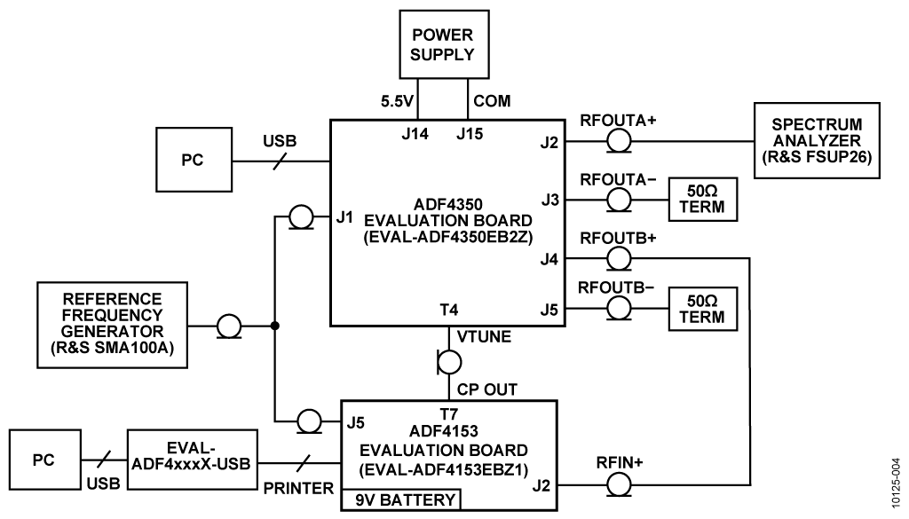
Functional Block Diagram
For this experiment, the EVAL-ADF4153EBZ1 and the EVAL-ADF4350EB2Z are used. The EVAL-ADF4350EB2Z is selected because it contains the auxiliary RFOUTB+ output stage, which is connected via SMA cable to the EVAL-ADF4153EBZ1, as shown in Figure 4.
Both PLLs use the same reference input (REFIN) frequency; therefore, an SMA splitter connects the same REFIN to both boards.
The loop filter output on the EVAL-ADF4153EBZ1 is connected to the VTUNE pin of the ADF4350 via a shielded coaxial cable to ensure that no extra noise or spurs appear on the pin. Both parts are programmed separately. It may be necessary to use different PCs for each board to ensure no conflicts occur between hardware drivers.
Getting Started
The UG-110 user guide details the installation and use of the EVAL-ADF4350EB2Z evaluation software. UG-110 also contains board setup instructions and the board schematic, layout, and bill of materials.
The UG-167 user guide contains similar information relevant to the EVAL-ADF4153EBZ1. Necessary modifications to the board are the removal of the VCO (Y1). To reconfigure this board as an input, remove the R7 resistor and change R8 and R9 to 0 Ω.
The PLL loop filter on the ADF4350 board is unused and should be removed. At this point, the microcoaxial cable can be used to connect the output of the ADF4153 loop filter (T7) to the VTUNE pin of the ADF4350 (T4). It is of critical importance that the outer shielding of this cable is connected to a ground point on both boards.

Initialization Procedure
The ADF4350 must go through the band select process for every new frequency.
- Initialize the ADF4350 as normal (program R5, R4, R3, R2, R1, R0), except set DB4, R2 to 1 (ICP three-state enabled), because the ADF4350 charge pump is unused. Set DB9, R4 to 0 for divided VCO output on RFOUTB+. Enable RFOUTB+ (auxiliary out). This signal is fed to the ADF4153 over the coax cable.
- Initialize the ADF4153 (as per the data sheet) to accept the VCO output frequency as the RF input frequency. Note that the band select switch is internal; therefore, an external switch to remove the PLL VTUNE is not required.
- When the ADF4153 achieves lock, the ADF4350 counter reset to 1 (DB3, R2) must be activated. Not activating the counter reset degrades spur performance. Additionally, all ADF4350 synthesizer blocks can be powered down using the test mode bit (DB10, R5).

Frequency Update
- Program DB10, R5 to 0 to reactivate the ADF4350 synthesizer blocks.
- Program DB3, R2 of the ADF4350 to 0 to deactivate the counter reset because these counters are required for band select.
- Program the ADF4350 and ADF4153 N-counter registers as
- When the ADF4153 achieves lock, the ADF4350 counter reset (DB3, R2) can be activated. Additionally all synthesizer blocks can be powered down using the test mode bit (DB10, R5).
- Repeat Step 1 to Step 4 as required for new frequencies.
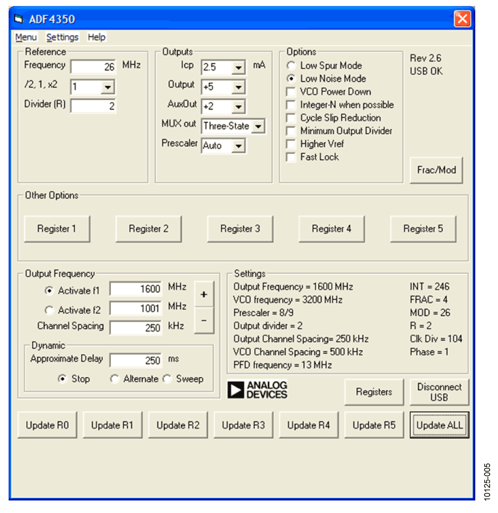
The software screen captures shown in Figure 5 and Figure 6 show the software windows for 26 MHz REFIN (ADF4350) and 13 MHz PFD (ADF4153). After setting up the equipment, use standard RF test methods to measure the spectral purity of the output signal.

