CN0148


Overview
Design Resources
Device Drivers
Software such as C code and/or FPGA code, used to communicate with component's digital interface.
AD7606 GitHub Linux Driver Source Code
AD760x GitHub no-OS Driver Source Code
AD7606 IIO Multi-Channel Simultaneous Sampling ADC Linux Driver
Features & Benefits
- Mutlichannel simultaneous sampling data acquisition system
- Layout guidelines for 16 bit performance
Product Categories
Markets and Technologies
Parts Used
Documentation & Resources
-
MT-021: ADC Architectures II: Successive Approximation ADCs2/14/2015PDF3799 kB
Circuit Function & Benefits
In power line measurement and protection systems, there is a requirement to simultaneously sample large numbers of current and voltage channels of multiphase power distribution and transmission networks. In these applications, the channel count can vary from as few as six channels to greater than 64 channels. The AD7606 8-channel data acquisition system (DAS) with 16-bit bipolar simultaneously sampling SAR ADCs with on-chip overvoltage protection greatly simplifies signal condi-tioning circuitry and reduces the overall parts count, board real estate, and cost of the measurement and protection board. Even with its high level of integration, each AD7606 requires only nine low value ceramic decoupling capacitors.
In measurement and protection systems, simultaneous sampling capability is needed to maintain the phase information between the current and voltage channels on multiphase power line networks. The wide dynamic range capability of the AD7606 makes it ideal for capturing both under voltage/current and over voltage/current conditions. The input voltage range is pin-programmable for either ±5 V or ±10 V.
This circuit note describes details of the recommended PC board layout for applications using multiple AD7606 devices. The layout is optimized for channel-to-channel matching and part-to-part matching and will help reduce the complexity of calibration routines in high channel count systems. The circuit provides the ability to use the AD7606 2.5 V internal reference when channel-to-channel matching is important or an external ADR421 precision high accuracy (B grade: ±1 mV max), low drift (B grade: 3 ppm/°C max), low noise (1.75 μV p-p, typical, 0.1 Hz to 10 Hz) reference for high channel applications that require excellent absolute accuracy. The low noise and the stability and accuracy characteristics of the ADR421 make it ideal for high precision conversion applications. The combination of the two devices yields a level of integration, channel density, and accuracy that is unsurpassed in the industry.
Circuit Description
The AD7606 is an integrated, 8-channel data acquisition system with input amplifiers; overvoltage protection; second-order analog antialiasing filters; analog multiplexer; 16-bit, 200 kSPS SAR ADC; and a digital filter—all included on-chip. The circuit shown in Figure 1 consists of two AD7606 devices configurable with the ability to use either the internal 2.5 V reference or an external 2.5 V ADR421 reference. When the REF SELECT pin is connected to a logic high, the internal reference is selected. When the REF SELECT pin is connected to a logic low, the external reference is selected.
The power supply requirements are as follows: AVCC = 5 V, VDRIVE = 2.3 V to 5 V (depending on external logic interface requirements).
This circuit note describes the layout and performance of an evaluation board that contains two AD7606’s, making a 16-channel data acquisition system. Complete 16-channel DAS PC board documentation is available at www.analog.com/CN0148_PCB_Documentation
Symmetrical layout around the analog input channels and device decoupling is important for good channel-to-channel matching and part-to part matching. Data is shown to support the matching performance obtainable with the 16-channel ADC shown in Figure 1.


Dual AD7606 Board Layout for 16-Channel DAS
In a system that contains multiple AD7606 devices, a symmetrical layout between the AD7606 devices is important to ensure good device-to-device performance matching. Figure 2 shows a layout with two AD7606 devices.


The AVCC supply plane runs to the right of both devices. The VDRIVE supply track runs to the left of the two AD7606 devices. The ADR421 reference chip is positioned between both AD7606 devices, and the reference voltage track runs upward to Pin 42 of U2 and downward to Pin 42 of U1. A solid ground plane is used. These symmetrical layout principles can be applied to a system that contains more than two AD7606 devices. The AD7606 devices can be placed in a north-south direction with the reference voltage located midway between the AD7606 devices and the reference track running in the north-south direction, similar to Figure 2.
Good decoupling is also important to lower the supply impedance presented to the AD7606 and to reduce the magnitude of the supply spikes seen by the AD7606 devices. The decoupling capacitors should be placed close to, ideally right up against, these pins and their corresponding ground pins. The decoupling capacitors for the REFIN/REFOUT pin and the REFCAPA and REFCAPB pins are critical performance capacitors and should be placed as close as possible to their respective AD7606 pins; where possible, they should be placed on the same side of the board as the AD7606 device. Figure 3 shows the recommended decoupling on the top layer of the AD7606 board. The four ceramic capacitors shown are the decoupling caps for the REFIN/REFOUT pin, REGCAP pins, and REFCAPA and REFCAPB pins. These capacitors are placed in a north-south direction to get as close to their respective pins as possible.


Figure 4 shows bottom layer decoupling. Bottom layer decoupling is for the four AVCC pins and the VDRIVE pin. Multiple vias are used to connect the pins to their respective decoupling capacitors. Symmetrical layout of the decoupling capacitors around the AD7606 devices will help with part-to-part performance matching. Multiple vias are used to connect capacitor pads and pin pads to ground and supply planes and the reference track.


Channel-to-Channel Matching for 16-Channel System
In high channel count systems good channel-to-channel and part-to-part performance matching will help to greatly simplify calibration routines. Symmetrical layout of the AD7606 devices, the analog input channels, and the decoupling capacitors will aid performance matching between multiple devices. The use of a common system reference will further enhance matching performance in the system. Figure 5 shows the circuit configu-ration used to measure channel-to-channel matching between the 16 channels on the board when all inputs are grounded. There is a maximum histogram spread of 7 codes with each channel histogram centered on code 0, as shown in Figure 6.


Using the AD7606 Internal Reference as the System Reference
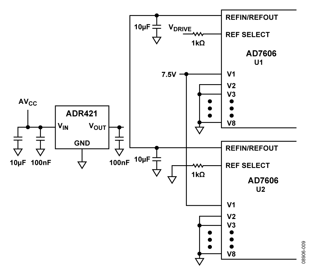
The AD7606 has an internal 2.5 V reference that is internally amplified to provide the AD7606 ADC with an approximate 4.5 V buffered reference. In high channel count applications where channel-to-channel and part-to-part matching performance is critical, the internal reference of one AD7606 can be used to provide the reference to the second AD7606 device. For this configuration, U1 is configured to operate with the internal reference enabled, as shown in Figure 7.


The AD7606 U2 device is configured to operate in the external reference mode. The 2.5 V reference available at the REFIN/RFOUT pin of U1 is routed to the REFIN/REFOUT pin of U2. A 10 μF decoupling capacitor is placed on the REFIN/REFOUT pins of the AD7606 devices. On both AD7606 U1 and U2, the REFCAPA and REFCAPB pins are shorted together and decoupled to GND using a 10 μF ceramic capacitor.
Both AD7606 devices are operating at a sampling rate of 200 kSPS, and a 7.5 V dc signal is applied to V1 and V2 of U1, as shown in Figure 7. The histogram of codes is recorded and shown in Figure 8. The difference in the mean output code was 1.2 codes between channels on the same device. All 16 channels on the board are converting at 200 kSPS.


The 7.5 V signal was applied to V1 of U1 and V1 of U2; all 16 channels on the board are operating at 200 kSPS, as shown in the simplified configuration circuit of Figure 9. The histogram of codes is recorded in Figure 10. The difference in the mean output code was 1.4 codes between V1 channels on different devices.


When using the internal reference of one AD7606 as the system reference, the above plots indicate that the channel-to-channel matching is very good between channels on a single device and between channels on multiple AD7606 devices.
Absolute Accuracy
When absolute accuracy of the ADC conversion result, in addition to channel-to-channel and part-to-part matching, is critical, an external tight tolerance low drift reference should be used as the system reference. In this circuit, the ADR421 2.5 V reference is used as the system reference.
The ADC output code will be influenced by the reference voltage applied to the AD7606 device:

The value for the actual ideal code will vary over temperature depending on the temperature coefficient specification of the system reference. In applications where absolute accuracy is important or in applications that wish to avoid complex temperature calibration routines for absolute accuracy and channel matching, a tight tolerance low drift 2.5 V reference like the ADR421 should be used as the system reference for the AD7606 devices.
A dc voltage of 7.5 V is applied to the input of U1 (V1 and V2), shown in the circuit of Figure 11, using the external reference. The histogram of codes of the two channels on U1 is recorded in Figure 12. The difference in the mean of the histogram of codes for both channels is 0.9 LSB.


The 7.5 V dc is applied to V1 channels on U1 and U2 AD7606 devices in the circuit of Figure 13 to test part-to-part matching using the external reference. The histogram of codes of the two V1 channels for two AD7606 devices is shown in Figure 14. All 16 channels on the board are running at 200 kSPS throughput rate. The difference in the histogram mean between the V1 channels on U1 and U2 is 0.6 LSB.


The histograms indicate that, with the ADR421 external system reference, the matching between the mean of the histograms on one AD7606 device and between multiple AD7606 devices is less than 1 LSB.
Conclusions
This layout ensures good channel-to-channel matching using a single AD7606 and also good part-to-part matching between multiple AD7606’s on the same PC board. Symmetrical layout around the AD7606 devices and, in particular, the decoupling capacitors will aid with channel-to-channel and part-to-part matching. Good channel-to-channel and part-to-part matching will mean less complex calibration routines in high channel count systems.
Common Variations
The AD7606 is an 8-channel DAS. Also available are the AD7606-6 (6-channel DAS) and AD7606-4 (4-channel DAS). The AD7607 is a 14-bit version of the AD7606. Alternate voltage references can be chosen using the Voltage Reference Selection and Evaluation Tool.