Measuring Skew Margin on 4-Channel Deserializers
Abstract
The skew margin of an LVDS deserializer is an indication of its jitter tolerance. This application note describes conditions that can limit skew margin, and it presents a procedure for measuring skew margin on 4-channel deserializers.
Introduction
The skew margin of an LVDS deserializer is an indication of its jitter tolerance. Application Note 3821: Skew Margin Measurement for 4-Channel (3 Data Channels Plus Clock Channel) LVDS Serializers/Deserializers demonstrates an approach for measuring skew margin by utilizing a serializer and LVDS interconnect. This application note describes how to measure skew margin utilizing only a deserializer. The outlined procedure can be used for virtually any LVDS deserializer.
Receiver Skew Margin (RSKM)
RSKM is a valid timing window in which a deserializer can correctly sample LVDS input data. To sample the data within the data-bit time (unit interval or UI), a timing strobe signal is generated from the LVDS input clock. Ideally, this strobe signal should be positioned in the middle of the data pulse, so the maximum RSKM can approach half of the LVDS data bit. However, many nonideal, internal and external conditions can reduce the available timing margin to the point where the sampling window closes and data "errors" develop.
Some of the internal chipset parameters that can limit RSKM are listed below:
- Deserializer internal strobe uncertainty, which is related to data setup and hold timing requirements
- Transmitter pulse position variation, which is the change in the position of individual serializer output data bits with respect to the serializer LVDS clock
Other RSKM-reducing factors are related to LVDS interconnect and include:
- Cable skew
- Intersymbol interference (ISI)
- Parallel input-clock jitter passed by the serializer to the deserializer
Improving RSKM
The main factors contributing to cable skew are cable length, cable type, and cable quality. The following design recommendations can be implemented to improve RSKM:
- Use short, high-quality cables with a low skew per unit length (10–20ps/ft). Note that the total skew path also includes the connector and PCB trace skew. Good quality connectors and good board layout practices (e.g. matched trace lengths) add little or no skew.
- The use of short cables, DC-balanced mode, and a line equalizer minimize the effect of ISI.
- Applying a clean input-clock signal to the serializer improves the jitter performance of the data/clock and maintains a good skew margin. Also, proper transmission line termination prevents reflections and assists in maintaining signal integrity and skew margin.
Recommended Equipment
Agilent™ 8133A pulse generator
Tektronix® CSA8000 or similar digital sampling scopes
Tektronix P6248 differential probe
Tektronix 1103 TEKPROBE BNC™ power supply
SMA cables
DC power supply
Test Procedure
- Configure the serializer in DC-balanced mode. Figure 1 shows the AC-coupled configuration, and
Figure 2 depicts the timing relationship between the clock and data.

Figure 1. The AC-coupled configuration of the MAX9242/44/46/54 deserializer in DC-balanced mode.

Figure 2. The timing relationship between the clock and data of the deserializer serial input in DC-balanced mode.
- Connect the Channel 1 differential outputs of the Agilent 8133A pulse generator to the RxIN0- and RxIN0+ inputs of the 4-channel deserializer (MAX9236, MAX9244, etc.) using equal-length cables. Follow these steps for proper setup:
- Choose a clock frequency of 32MHz
- Select pulse mode
- Use an 11.1% duty cycle (1/9)
- Use the COMP key (compliment of the signal)
- Use the following signal levels: High = 1.5V, Low = 1.0V (DC Offset = VCM = 1.25V)
- Connect the Channel 2 differential outputs of the Agilent 8133A pulse generator to the RxCLKIN+ and RxCLKIN- inputs of the deserializer. Use the same signal levels, and follow Steps 2a–2e.
Figure 3 presents the data and clock signal waveforms that result from following the procedure described in Steps 1–3.

Figure 3. Data and clock signal waveforms produced by following test-setup Steps 1–3.
- Use a differential probe to measure the clock with the available sampling scope. Then, connect the same probe to the deserializer’s differential data input for the following measurements:
- Figure 4 demonstrates that the clock and data are not initially aligned. Ideally, the clock and data should cross at the differential ground. If this is not the case, add delay to the data until it is aligned with the clock. Use the "delay" option on Channel 2 of the Agilent 8133A pulse generator. Call it "delay offset".
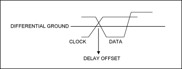
Figure 4. Misalignment/offset between the clock and data.
- Monitor the RxOUT0 pin of the deserializer. During normal operating conditions, this pin should be at the level of VCC.
- Increase the data delay while monitoring the level of RxOUT0 with a multimeter. Record the delay value as soon as the RxOUT0 signal transitions from 1 to 0. Call this: "+ delay".
- Next, decrease the delay to the negative region, and record the delay again when RxOUT0 transitions from 1 to 0. Call this: "- delay".
- Subtract the delay offset from "+ delay". This is called "RSKM-". Add the delay offset to "-delay". This is called "RSKM+". Figure 5 shows the RSKM- and RSKM+ regions with respect to the internal strobe signal of the deserializer.
- Ideally, RSKM+ and RSKM- should be identical; however, in reality they are always different. Note that the closer RSKM+ and RSKM- are to the same value, the better the skew margin for the device.

Figure 5. RSKM-, RSKM+, and strobe signal relationship.
- Figure 4 demonstrates that the clock and data are not initially aligned. Ideally, the clock and data should cross at the differential ground. If this is not the case, add delay to the data until it is aligned with the clock. Use the "delay" option on Channel 2 of the Agilent 8133A pulse generator. Call it "delay offset".