How to Install MAX44211 Output Protection
Abstract
The internal ESD clamping structure is present to protect the MAX44211 from ESD and other sub-microsecond events. When the application has hazards where these events can occur frequently and for comparatively longer time, it is recommended to use external protection circuitry. This application note describes how to add this protection circuitry on the MAX44211.
How to Install MAX44211 Output Protection
Unwanted transients emanating from the power line back to the line-driver's output and back-EMF generated by the coupling circuit when the load is disconnected and connected, and vice versa, create undesirable overvoltage conditions. Back-EMF is also generated when the line driver outputs are toggled from high to low impedance state, if significant current was flowing at the disconnect time. The MAX44211 power line communications driver most often is placed facing the power line with an isolating stage between them. In case of such overstress conditions, external protection is required to protect the MAX44211 and downstream circuits.
The internal ESD clamping structure is present inside MAX44211 (see Figure 1) to protect the part from ESD or sub-microsecond events. When the application has hazards where these events can occur frequently and for comparatively longer time, it is recommended to have external protection circuitry. Failure to accommodate an output protection can result in overstressing the outputs (OUT+/ OUT-) and eventually damage the part.
This application note provides insights and information on how to add external protection circuitry at the outputs of the MAX44211. A circuit using VAVDD = 15V is used in this application note.
Figure 1 shows the internal ESD clamping protection structure.

Figure 1. Internal ESD clamping protection structure.
Absolute Maximum Ratings at the Outputs
OUT+, OUT- to GND: VGND - 0.3V to (VAVDD + 0.3V)
The internal ESD protection diodes are P-N junction diodes. To prevent normal conduction over the full operating temperature range, these diodes should not be forward-biased by more than 300mV. At this level, the leakage across the internal P-N diode is still negligible. At room temperature and approximately 0.6V to 0.7V, the forward current across the diode increases. Eventually increasing the voltage limit on the diodes increases its forward current exponentially, eventually damaging the device.
The ESD protection for the MAX44211 is designed to withstand approximately ±2.5kV pulses for 150ns according to the JEDEC JESD22-A114 standard. In any case, attempting to expose the outputs for higher voltage beyond the absolute maximum ratings for more than 150ns is considered violating the abs max. See Figure 2 for the output protection structure.
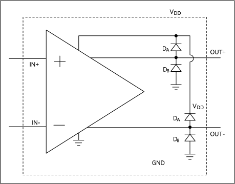
Figure 2. Output protection structure.
Surge Test and Quasi-DC Test
Two tests, surge tests and quasi-DC, were done to understand the characteristics of the internal output clamping diodes. The surge test forces overvoltage conditions for a shorter time compared to the quasi-DC test, so the surge test is expected to carry more current through the diodes. Tests were done at +25°C and +85°C.
Surge Test
For the surge test, a stand-alone diode was tested by applying a surge pulse as per 61000-4-5 IEC standard. This pulse was of triangular shape (tR ~1.5µs) and with duration ~100µs. Figure 3 shows surge test characteristics.

Figure 3. Test surge characteristics.
Quasi-DC Test
For the quasi-DC test, a stand-alone diode was tested by applying a quasi-DC test using Keithley 2410 sourcemeter. This pulse was of trapezoidal shape (tR ~10µs) and with duration ~350µs.

Figure 4. Quasi-DC test signal.
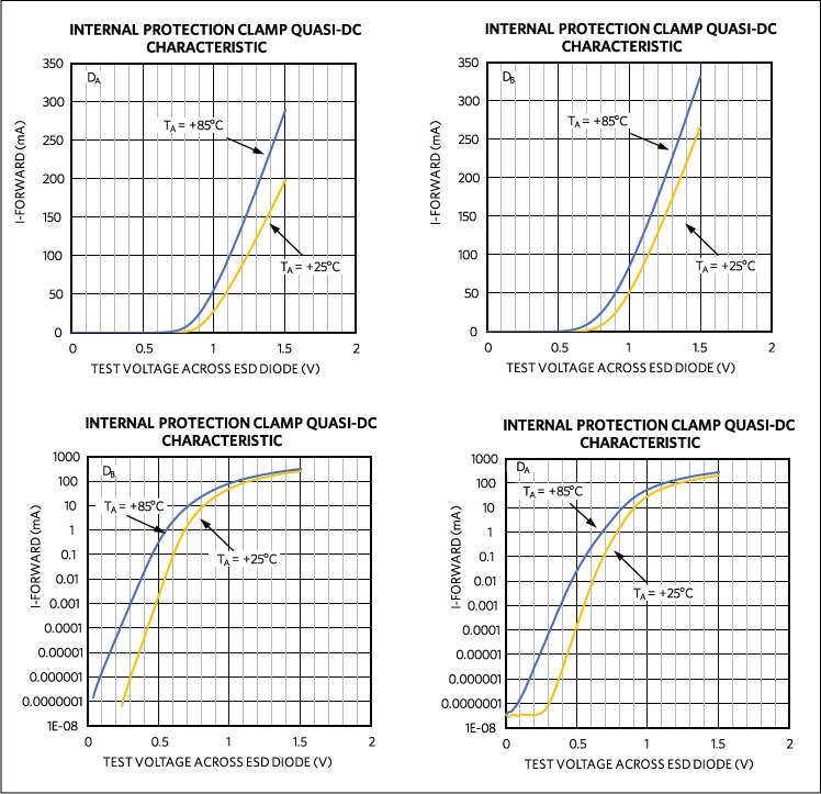
Figure 5. Internal protection clamp quasi-DC characteristics.
Observations from the Surge and Quasi-DC Tests
- The internal clamping diode DA carries 1mA (in the region of turn-on knee) at 0.78V at +25°C and 0.7V at +85°C.
- The internal clamping diode DB carries 1mA (in the region of turn-on knee) at 0.7V at +25°C and 0.55V at +85°C.
- The behavior of DA (anode signal to cathode AC ground) and DB (cathode signal to anode AC ground) is asymmetrical because of a minute internal structural difference.
- The clamping diode DB (cathode signal to anode AC ground) can comparatively take more current than DA.
- The clamping behavior is going to be at a higher votlage for the internal diodes at a lower temperature like -20°C or -40°C.
External Protection Solution
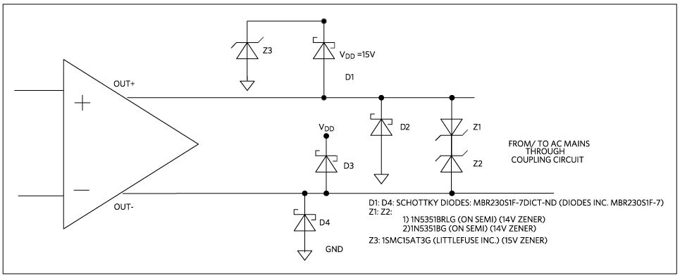
Figure 6. External protection.
Table 1 shows the component information. A Using Zener diodes for Z1 and Z2 instead of a standard TVS transorb is preferred because even though TVS diodes absorb comparatively a large amount of energy during transient events, their voltage cutoff points are not finely controlled and age with time. The Zener diode offers a well-defined clamping voltage. Bidirectional operation is achieved by using the Zener diodes in a back-to-back configuration.
The role of Z3 is to clamp the voltage across VDD to GND to 24V. D1:D4 and Z2 and Z3 provide an additional defense in case of overvoltage stress. D1:D4 bypass the fault currents to the supply plane and the Z1 Z2 combination bypasses the fault currents at the output traces and back into the power line, thereby protecting the OUT+ and OUT- outputs. Expected clamping voltage from the back-to-back Zener diodes = 14V + 0.7V = 14.7V.
| Component | Component code | Component type | Description |
| D1:D4 | MBR230S1F-7DICT-ND | Schottky diode | 850mW, 30V 2A |
| Z1:Z2 | MMSZ4701T1G | Zener diode | 500mW, 14V clamp |
| Z3 | 1SMC15AT3G | Zener diode | 15V reverse standoff, 24V clamp, 1.5kW (peak pulse) |
Test Description
VDD is set to 15V constant. VTEST is ramped discretely from 0 to 16V to observe when the Zener clamp kicks in and when the Schottky turns on. It was made sure that the VTEST signal was "ON" for 1-2 seconds before turned off and observations were made during the “ON” condition. This was done to make sure the continuous power dissipation over time is negligible. The test was carried out at -30°C, +25°C, and +60°C.
When the VTEST signal is beyond 15V, the current across the Zener clamping diodes rises exponentially and, thereby, the power dissipated rises beyond 500mW. The Z1 and Z2 Zener diodes are rated only for 500mW continuous PDIS. So, the above protection feature is intended only for an instantaneous and not continuous purpose, as is expected during power line transient events.
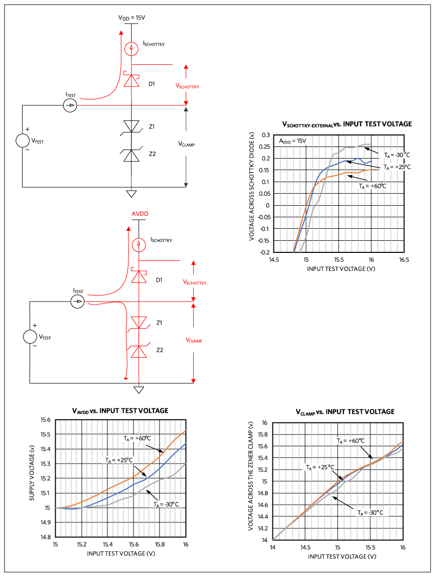
Figure 7. Test setup and results for the external protection solution.
Observations from the External Protection Solution
- When the external Schottky diodes are turned on, current flowing to AVDD tries to pull the AVDD voltage closer to the signal voltage.
- The Zener back-to-back clamps are the first line of defense. They turn on first before the Schottky diodes turn on.
- For the same test conditions, the Schottky's clamp voltage is less at hot and more at cold temperatures.
- The VCLAMP or Zener clamp voltage tracks close over temperature as seen above.
- From the above observations, we can infer that:
- The two layers of protection turn on and make sure the internal diodes do not turn on.
- Even in the event the internal diode turns on (briefly), most of the current is bypassed through the Schottky and the Zener clamp, thereby protecting the line driver’s internal diode. The characteristic of internal clamps can be observed from the quasi-DC test.