How to Increase the Operating Speed on the MAX4007
Abstract
The MAX4007 is a precision, high-side, high-voltage current monitor specifically designed for monitoring photodiode current in fiber applications. This application note describes a simple way to increase the MAX4007's response time for GPON burst-mode operation.
Description of Operation
The MAX4007 is a current monitor that outputs a current proportional to that flowing out from its REF pin. If the output is to be sampled by an ADC, however, the output must be first converted to a voltage. A simple way to achieve this is by using an output resistor in parallel with a 10nF anti-aliasing capacitor. This arrangement (Figure 1) can be seen in the device's data sheet.

Figure 1. MAX4007 application example.
Having an output resistor in this configuration loads the output of the current monitor, causing its response to slow, whether or not an anti-aliasing capacitor is present. An easy way to overcome this limitation is to substitute the output resistor with an output transimpedance amplifier. This change eliminates the loading effect at the MAX4007's output, and increases its operating speed substantially. This design approach is very useful for GPON burst-mode controllers that need response times in 100's of nanoseconds.
To better illustrate the difference between the two approaches, we will examine an example circuit. Figure 2 shows a circuit that can be used to test the basic functionality of the MAX4007.

Figure 2. This circuit tests the operating speed of the MAX4007.
Figure 2 shows a sample circuit that can be built to test the MAX4007 in high-voltage applications, such as those required for APDs. This concept can also be applied to PIN photodiodes or other low-voltage photodetectors. The input circuit is composed of VIN and Rt and Ri, which are connected to simulate the effect of a switching current source, as a photodiode would behave. Since VIN is created with a function generator with a maximum voltage swing of ±5V, a 20V power supply was used as a reference to the function generator so that the circuit could be tested at a BIAS voltage of 25V. Ci1, Ci2, Cf1, Cl1, and Cl2 are present for filtering and do not interfere with the normal operation of the circuit. Component and VIN values are chosen to generate a current step from 1mA to 10µA. Figure 3 shows the circuit response in this configuration.

Figure 3. Data show the MAX4007's response if a resistor is used as output device.
As the curve in Figure 3 shows, this is the same type of response expected from the device as specified in the data sheet.
If we now replace the passive output components for the circuit, we can greatly improve the MAX4007's response time. See Figure 4.

Figure 4. MAX4007 in a configuration with an output operational amplifier.
Figure 5 shows the large signal impulse response of the MAX4007 when a 10µA to 1mA current step is applied to the REF pin. The time constant for rising pulse is about 57ns, and 26ns for the falling pulse.
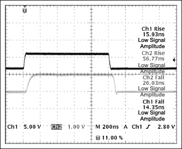
Figure 5. The MAX4007's response with output operational amplifier.
The end application in Figure 4 is extremely small with one SOT23 device (MAX4007), an opamp in an SC70 package (MAX4412), and a few discrete components.