How to Add Reverse Current to the MAX15090B/MAX15090C for Hot-Swap with Integrated FET Applications
How to Add Reverse Current to the MAX15090B/MAX15090C for Hot-Swap with Integrated FET Applications
Abstract
The MAX15090B/MAX15090C ICs provide overvoltage and undervoltage protection and current limiting, but do not include reverse current protection. This application note provides guidelines on how to add reverse current protection when using these ICs.
Introduction
The MAX15090B/MAX15090C ICs are 12A rated integrated solutions for hot-swap applications requiring the safe insertion and removal of circuit line cards from a live backplane. The devices integrate a hot-swap controller, 6mΩ power MOSFET, and an electronic circuit-breaker protection in a single 2.07mm x 3.53mm WLP package. This integrated small package makes the devices ideal for space-constrained designs. They provide overvoltage protection, undervoltage protection, and current limiting, but do not include reverse current protection. Reverse current protection is sometimes necessary to prevent current flowing from output to input when the part is disabled. This application note describes how to add reverse current protection.
What is Reverse Current Protection?
There are essentially two forms of reverse current protection in a current limited switch. A common form of reverse current protection is when the electronic fuse switch is open (disabled) and the output voltage is greater than the input voltage. Figure 1 shows a basic diagram where the reverse current path in a typical current-limited hot-swap IC with integrated switch is not reverse current protected. With voltage present at the output, the internal body diode provides a current path to the input even when the internal pass FET is disabled.
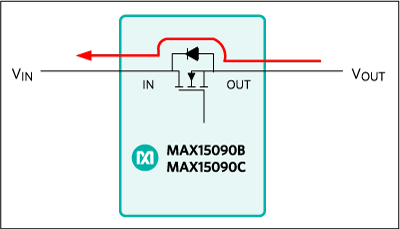
Figure 1. Reverse current flowing through body diode when VOUT > VIN (FET disabled).
Why is reverse current bad? Consider an application where the input power source is a battery. When the switch is disabled, if for some reason (due to the application circuit) there is power on the output side, there is a potential for destructive current flowing back to the battery. Another case would be if there is a battery backup source on the output side that supplies current to the application load when main input power is lost. In this case it would be undesirable to have current flowing back to the input draining the battery and a potential to provide an overcurrent discharge path from the battery. Additionally, the current discharge path through the body diode can also be destructive.
The power dissipation across the body diode is expressed as PDIODE = IREVERSE CURRENT x diode voltage drop. Depending on the magnitude of the reverse current, the internal power dissipation inside the device results in an unwanted temperature rise, where the heat generated exceeds the thermal rating of the device, thereby leading to combustion and device destruction.
The other mode of reverse current protection not only blocks reverse current from flowing back to the input when the eFuse is disabled, but it provides reverse current protection when the device is enabled. In this scenario, the protection element would need to monitor the difference between VIN and VOUT and, if the voltage at VOUT becomes positive relative to VIN, the main pass FETs are quickly disabled, preventing reverse current that could damage the pass element. No attempt is made in this application note to add extra circuitry for this function to the MAX15090B/MAX15090C. Maxim offers ICs like the MAX17523, MAX17525, MAX17561, MAX17562, and MAX17563 that provide reverse current protection when the device is enabled.
Driving the External FET
Because the MAX15090B/MAX15090C provide access to the internal GATE signal, it is possible to add an additional NCH MOSFET to form a back-to-back to FET configuration to block the reverse current path when the VIN to VOUT connection path is disabled. There are several requirements in selecting the FET. The gate charge current is 4.5µA and the internal charge pump generates 4.5V above VIN to enhance the pass FET. As such, two of the main FET requirements are IGSS (gate body leakage) and VGS(TH) (gate threshold voltage). Additionally, VDSS (drain to source voltage rating) and VGSS (gate to source voltage) ratings should be considered. In looking at various options the FDMS8333L was chosen. The published IGSS is ±100nA and the VGS(TH) gate threshold is typically 1.8V. Additionally, the VDSS and VGSS ratings of 40V and ±20V are more than enough for safe operation. Another important parameter to consider is RDS(ON). Because the typical RDS(ON) = 3.3mΩ for this device, typical power dissipation at 12A is only 0.475W! Figure 2 shows the schematic of the finished circuit with reverse current protection.
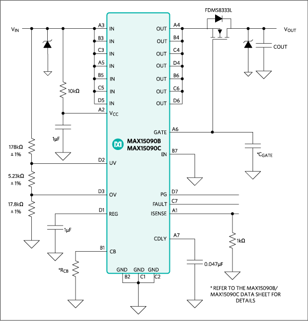
Figure 2. MAX15090B/MAX15090C with reverse current protection.
Conclusion
In certain circuit applications where a hot-swap function with current limiting is required, it is mandatory to have reverse current protection. Most higher current hot-swaps with integrated FETs do not offer reverse current protection! Typically, designers needing a higher current hot-swap function with reverse current protection only choice has been to use a hot-swap controller. This approach requires two external FETs and a current-sense resistor. Since the MAX15090B/C ICs provide access to the gate control pin, it is possible to add reverse current protection by simply adding a single external FET. Since the MAX15090B/C current sensing is internal, additional space savings are realized as the need for the external current-sense resistor is eliminated.