DS31256 PCI Bus Utilization
Abstract
This application note explains how to calculate the bus bandwidth for the DS31256 HDLC controller. Lab-test examples are shown. The Bus Utilization Calculator spreadsheet is explained and is available upon request.
Overview
The DS31256 HDLC Controller accesses the PCI bus to obtain and store HDLC packets as they are sent and received. This application note explains how to calculate how much available bus bandwidth the DS31256 will require to operate properly. Terms used throughout this application note will be defined at the outset.
With the information provided in this application note, the user can modify the numbers in the calculator spreadsheet (available upon request) to fit their particular application.
| Variable | Definition | Valid Range |
| B | Average number of packets processed before the host updates the receive free queue and transmit pending queue or reads the receive done queue and transmit done queue | 1, 2, 3, . . . . |
| C | Average number of bus cycles required per packet | 1, 2, 3, . . . . |
| D | Number of bus cycles needed for data to be transferred | 1, 2, 3, . . . . |
| P | Packet size in bytes | 64 |
| R | Average number of bus cycles added due to latency in RAM access | 0, 1, 2, . . . . |
| X | Average number of bus accesses required to send or obtain packet data to, or from the data buffers | 1, 2, 3, . . . . |
Types of Bus Access
The DS31256 or the host performs four types of bus access to support the Direct Memory Access (DMA) in the DS31256. In the following descriptions, the variable D is defined as the number of data cycles, and the variable R is defined as the number of bus cycles needed due to RAM access latency.
Access Type 1: Burst Read by the DMA from the Host RAM
The total number of bus cycles required when the DMA burst read from the host RAM is [3+R+D]. This equation was derived from Figure 1 and Table 2.
| Cycle | No. Cycles Required |
| Address Cycle | 1 |
| Turnaround Cycle | 1 |
| RAM Access Latency Cycle | R |
| Data Cycle | D |
| Turnaround Cycle | 1 |

Figure 1. DS31256 PCI bus read.
Access Type 2: Burst Write by the DMA to the Host RAM
The total number of bus cycles required when the DMA burst write to the host RAM is [2+R+D]. This equation was derived from Figure 2 and Table 3.
| Cycle | No. Cycles Required |
| Address Cycle | 1 |
| RAM Access Latency Cycle | R |
| Data Cycle | D |
| Turnaround Cycle | 1 |

Figure 2. DS31256 PCI bus write cycle.
Access Type 3: Write by the Host to the DS31256
The total number of bus cycles required when the host writes to the DS31256 is 7.
Access Type 4: Read by the Host to the DS31256
The total number of bus cycles required when the host reads from the DS31256 is 7.
Note: For access Types 3 and 4, the 7-cycle access is inherent to the DS31256 and cannot be changed.
Number of Bus Cycles Needed per Packet
To calculate bus utilization, the number of required bus cycles must be known. To obtain this number, several assumptions are made and listed in Table 4. Figure 3 shows the standard sequence that the host and DMA will follow for each packet received or transmitted. From Figure 3, it is possible to create a formula to calculate the average number of bus cycles required per packet, which is the variable C.
Transmit Side
Cycle of Transmit Side = Read Pending Queue + Write Horizontal Descriptor Chaining + Read Descriptor + Read Packet from Host Memory + Write Done Queue + Read/Write Registers.
Ct = [(3 + R + 12)/12] + [2 + R + 1] + [3 + R + 4] + [(P/4) + (3 + R)X] + [(2 + R + 6)/6] + [4(7/B)]
Receive Side
Cycle of Receive Side = Read Free Queue + Write Packet to Host Memory + Write Descriptor + Write Done Queue + Read/Write Registers.
Cr = [(3 + R + 24)/12] + [(P/4) + (2 + R)X] + [2 + R + 3] + [(2 + R + 6)/6] + [4(7/B)]
Total Formula
Ct + Cr = 21.16 + 3.5R + 0.5P + (5 + 2R)X + 56/B
| 1 | All packets are 64 bytes (seen as worst case). |
| 2 | The Frame Check Sequence (FCS) of the HDLC packet is not transferred to, or from the PCI bus. |
| 3 | On the receive side, only large buffers are used (small buffers are disabled). |
| 4 | The receive DMA will burst read the free queue and burst write the done queue. |
| 5 | The transmit DMA will burst read the pending queue and burst write the done queue. |
| 6 | All packets fit within a single buffer (i.e., only one descriptor). This is reasonable because packets are 64 bytes. |
| 7 | All physical layer links are filled with packets; no idle codes are sent or received. |
| 8 | Interrupt routines and overhead (like accesses to the local bus) are not considered. |

Figure 3. Bus cycle flowchart per packet.
Notes:
- 12 descriptors x 1 dword = 12 transmit pending-queue descriptor dwords
- Packet data in bytes = 4 bytes/data cycle
- 6 descriptors x 1 dword = 6 transmit done-queue descriptor dwords

Figure 3. (Continued)
Notes:
- 12 descriptors x 2 dwords = 24 receive free-queue descriptor dwords
- Packet data in bytes = 4 bytes/data cycle
- 6 descriptors x 1 dword = 6 receive done-queue descriptor dwords
PCI Bus Utilization
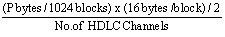
Bus utilization is defined as the number of bus cycles required by the DS31256 per second divided by the total number of bus cycles available per second. Bus utilization can be calculated for a specific HDLC configuration and traffic load. The calculation assumes that the PCI-bus clock rate is 33MHz (33,000,000Hz) and that one DS31256 is being used. Below are the detailed calculations of PCI bus utilization.
Formula 1:

Formula 2:

Notes:

Examples
The PCI Bus Utilization lab test was done to characterize the DS31256's PCI bus utilization. It was assumed that all the incoming and outgoing packets were 56 bytes long (P = 56). The results are summarized in Table 5. A spreadsheet that calculates the bus utilization (as shown in Table 6) is available upon request. (Please contact Analog Tech Support Team)
| B | P | R | |||||||
| Mode | No. of Ports | Avg. No. Done Queues Entries Processed | Pkt Size (Bytes) | Avg. RAM Access Latency Cycles | No. of HDLC Channels | Total No. of Channels | Channel Data Rate (kbps) | PCI Clock Rate (MHz) | PCI Bus Util.(%) |
| High Speed | 3 | 14.17 | 56 | 8.35 | 1 | 3 | 52 | 52 | 47.55 |
| Unchannelized | 3 | 35.53 | 56 | 8.50 | 1 | 3 | 29 | 29 | 49.06 |
| Low Speed | 16 | 100.46 | 56 | 10.60 | 1 | 16 | 12 | 12 | 55.27 |
| Unchannelized | 16 | 24.30 | 56 | 10.24 | 1 | 16 | 10 | 10 | 52.54 |
| T1 | 16 | 8.081 | 56 | 7.1375 | 12 | 192 | 128 * | 1.544 | 18.26 |
| E1 | 16 | 8.154 | 56 | 7.8645 | 16 | 256 | 128 | 2.048 | 28.07 |
| 2E1 | 16 | 10.894 | 56 | 8.003 | 16 | 256 | 256 | 4.096 | 55.82 |
| 4E1 | 16 | 381.207 | 56 | 8.3123 | 8 | 128 | 1024 | 8.192 | 50.97 |
* Notes:
|
|||||||||
| Input Variables | ||
| B | 14.17 | The average number of packets processed before the host updates the Receive Free Queue and Transmit Pending Queue, or reads the Receive/Transmit Done Queues. |
| P | 56 | The size of the packet in bytes. |
| R | 8.35 | The average number of bus cycles added due to latency in RAM access. |
| Number of HDLC channels per DS31256 | 3 | Use 1 per active port when operating in unchannelized mode. |
| Channel Data Rate (kbps) | 52,000.00 | Note that T1 speed == 1536kbps. |
| Channel Utilization Rate | 39.5% | There can be time between packets in real applications. |
| PCI Clock Rate (MHz) | 33 | |
| PCI Latency/Transaction | 10 | This is based on the average number of cycles required to perform each of the transactions associated with processing a packet. Our designers use 10 in their simulations, which is fairly conservative. |
| Number of DS31256's on Bus | 1 | |
| Intermediate Variables | ||
| C | 104.04 | The average number of bus cycles required per packet. |
| X | 1.00 | The average number of bus accesses required to send/obtain packet data to/from the data buffers. |
| Packets/second/channel | 45,871.43 | |
| Total PCI Latency | 1,376,142.86 | |
| No. of Bus cycles required/sec | 15,693,122 | |
| Half Duplex | Full Duplex | |
| Bus utilization | 47.6% | 95.11% |
| Bus Capacity (Mbps) | 264 | |
| Bus Throughput (Mbps) | 125.54 | 251.09 |
Note :
Where 1024 blocks is the FIFO size and the FIFO high and low watermarks are set to 50%.
Conclusion
This application note explains how to calculate the bus bandwidth required by the DS31256 for a given application. Some lab-test examples are provided. The spreadsheet to perform the calculation is available upon request.
If you have further questions about the HDLC controller products or you would like to request the PCI Bus Utilization Calculator spreadsheet, please contact the Analog Tech support team