Working with MAX9217/MAX9218/MAX9247/MAX9248/MAX9250 Evaluation Boards
Abstract
This application note describes how to prepare and use the evaluation boards for the MAX9217/MAX9247 serializers and the MAX9218/MAX9248/MAX9250 deserializers.
General Description
The MAX9217/MAX9218/MAX9247/MAX9248/MAX9250 evaluation boards (EV kits) are available for customer evaluation. These EV kits consist of two sections: The right half contains one of the single-channel serializer components (MAX9217 or MAX9247) and the left half contains one of the single-channel deserializer components (MAX9218, MAX9248, or MAX9250).
The EV kits require three clock signals, which can be supplied by the same source. The serializer works with two clock signals: PCLK and DE_IN, where DE_IN is normally divided by a factor of 16 or 32 of the PCLK. The deserializer section needs a REFCLK, which can come from the same source, or it can be provided by an independent local oscillator that is within 2% accuracy of the PCLK.
Steps to Prepare the EV kits
- Configure the EV kits (Figures 1 and 2) by setting the jumpers according to the configuration tables below (Tables 1–4).
- Apply power to the EV kit. A single 3.3V DC power supply is sufficient to support each section of the EV board; however, if component characterization is desired, it is recommended to supply separate sources for each of the component's power-supply pins (Table 2).
- Connect the PCLK, DE_IN, and REFCLK clock signals to the EV kit, as explained in Step 2 (also see examples below). An Agilent™ 8133A pulse generator is a good choice for providing all three clock signals from one source.
- Apply the input data to the input pins of the serializer (located at the right-half section of the EV kit) and check the deserializer output pins using a logic analyzer and a multimeter. A liquid-crystal display (LCD) can be used if the input to the serializer is a video signal, such as UNIGRAF's VTG-4116 video test patterns.
- Special attention should be given to jumper JP13 on the serializer board. By connecting this jumper to DVCC, the ground pins of JP17–JP21 (10 × 2 headers) are connected to 3.3V, and a fixed data pattern can be applied to the data inputs of the MAX9217/MAX9247 serializers. When external data patterns are applied, this jumper should be connected to ground.
Pseudorandom-Bit-Sequence (PRBS) Data Generation by the MAX9217/MAX9247
The MAX9217/MAX9247 can generate PRBS data for eye-diagram measurements by using the following configuration:
- Connect the active-low PWRDWN pin to ground.
- Connect both MOD0 and MOD1 pins (for the MAX9247, these pins are called I.C. and PRE) to a negative 2.5V DC voltage. The serializer eye diagram can be observed by connecting a differential probe to pins 2 and 3 of JP14/JP24 (4-pin, single-row headers) on the serializer board. The deserializer eye diagram is available on pins 2 and 3 of JP5/JP6 (4-pin, single-row headers) of the deserializer board.
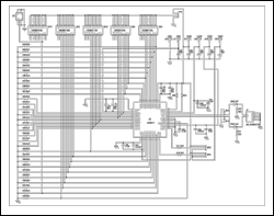
Figure 1. Circuit schematic for the MAX9217 EV kit.
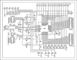
Figure 2. Circuit schematic for the MAX9218 EV kit.
Quick Functionality Check
The MAX9217/MAX9247/MAX9218/MAX9248/MAX9250 EV kits have headers for connection to a logic analyzer, a graphics generator, or a display. A pattern generator (which can be a part of the logic-analyzer system) such as the HP16500C system generates parallel test words that are applied to the serializer input. The test words are serialized and sent over the LVDS link to the deserializer. The logic analyzer then reads the deserialized test words and checks for errors against the reference or test words that were sent across the serializer and deserializer. The EV kit can also be connected to a graphics generator and LCD for a visual test of the serial link.
The basic function of the serial link can be checked without a logic analyzer, a graphics generator, or a display. For a quick check of the setup, the serializer input-logic levels can be set with jumpers, and the corresponding bits/voltages can be read with a voltmeter at the deserializer output. To configure the EV kit for a quick functionality check, refer to the MAX9217/MAX9218 EV kit schematics for the name and location of associated jumpers and components. Note that when a shunt is installed across a jumper pair, the chip pin is pulled to a logic-high level. If no shunt is installed across any jumper pair, the chip pin is pulled low.
- Configure jumpers for a quick functionality check of the EV kit (Table 1).
| Part | Pin Name | Jumper | Jumper Function | Jumper Setting for Quick Check |
| MAX9218, MAX9248, MAX9250 |
R/F | JP1 | Selects rising- or falling-edge output strobe | Low (falling edge) |
| RNG1 | JP4 | Selects PLL operating range | High-frequency range (refer to the data sheet) | |
| RNG0 | JP7 | Selects PLL operating range | High-frequency range | |
| Active-low PWRDWN | JP11 | Selects chip power-up or power-down | High (power-up) | |
| OUTEN (MAX9218/MAX9250), SS (MAX9248) | JP12 | Selects output enable or output disable | High (output enabled for MAX9218/MAX9250), 4% spread-spectrum mode (MAX9248) | |
| MAX9217, MAX9247 | (none) | JP13 | Buses logic high (DVCC) for hardwired inputs | DVCC |
| MOD1 (MAX9217), PRE (MAX9247) | JP15 | Selects output-modulation level | Low (modulation off), preemphasis is disabled for MAX9247 | |
| MOD0 (MAX9217), I.C. (MAX9247) | JP16 | Selects output-modulation level | Low (modulation off), internally connected pin for MAX9247 | |
| Active-low PWRDWN | JP18 pin 15 to pin 16 | Selects chip power-up or power-down | High (power-up) | |
| RNG0 | JP22 | Selects PLL operating range | High-frequency range (refer to the data sheet) | |
| RNG1 | JP23 | Selects PLL operating range | High-frequency range |
- Connect power supplies to the EV kit (Table 2).
| Part | Pin Name | EV Board Connection | Voltage |
| MAX9217, MAX9247 |
VCCIN | IVCC | +3.3V |
| VCCPLL | PVCC | +3.3V | |
| VCCLVDS | LVCC | +3.3V | |
| VCC | DVCC | +3.3V | |
| (none) | VNEG | Ground | |
| PLL GND, LVDS GND, GND | GND | Ground | |
| MAX9218, MAX9248, MAX9250 |
VCCPLL | PVCC | +3.3V |
| VCCLVDS | LVCC | +3.3V | |
| VCC | DVCC | +3.3V | |
| VCCO | OVCC | +3.3V | |
| (none) | VTEST | Open | |
| PLL GND, LVDS GND, VCCOGND, GND | GND | Ground |
- Connect all clock and control signals (Table 3).
| Chip | Chip Pin Name | EV Board Connection | Signal |
| MAX9217, MAX9247 |
PCLK_IN | J18 PCLK (SMA connector) | 32MHz |
| DE_IN | JP18 Pin 13 | 1MHz | |
| RGB_IN and CNTL_IN | JP18, JP19, JP20, JP21 | Open | |
| MAX9218, MAX9248, MAX9250 |
REFCLK | J8 REF (SMA connector) | 32MHz |
- Once Steps 1–3 have been completed, the following signals can be observed at the outputs of the MAX9218/MAX9248/MAX9250 deserializers (Table 4).
| Pin Name | EV Board Connection | Signal |
| RGB_OUT, CNTL_OUT |
JP3 and JP9 | Low |
| Active-low LOCK | JP9 Pin 23 | Low |
| PCLK_OUT | JP9 Pin 25 | 32MHz |
| DE_OUT | JP9 Pin 21 | 1MHz |
- The MAX9217/MAX9247 RGB_IN and CNTL_IN inputs have internal pull-down resistors. When an input is left open, the serializer automatically reads a logic low. Connect some inputs to 3.3V at the JP11, JP12, JP13, and JP14 headers. This can be done by setting JP13 to the DVCC position and using shunts between opposite pins of these 2 × 10 headers. The corresponding outputs on the MAX9218/MAX9248/MAX9250 deserializer should then change to a high level. For example, if RGB_IN0 (JP14 pin 1) is connected to 3.3V, then RGB_OUT0 (JP7 pin 27) should go high.
- Use an oscilloscope to view the serial signal by connecting a differential FET probe across the LVDS signal lines at the MAX9217/MAX9247 serializer outputs (JP17/JP18) or the MAX9218/MAX9248/MAX9250 deserializer inputs (JP4/JP6).
Notes
- RNG0 and RNG1 have internal pull-down resistors on the MAX9217/MAX9247 and MAX9218/MAX9248/MAX9250. To activate a logic low, these pins can be left floating.
- DE_IN must be switching for the MAX9217/MAX9218 chipset to work. Typically the Data Enable pin (ENAB) from a graphics controller is connected to DE_IN on the MAX9217/MAX9247 and is recovered from DE_OUT on the MAX9218/MAX9248/MAX9250. DE_IN must transition at least once every 4,194,304 cycles of PCLK_IN.
- The clock inputs have pads for 50Ω termination resistors to ground. The EV kit is shipped without these resistors—they are not installed. Clean transitions are especially important on the PCLK, DE_IN, and REF inputs. Install 50Ω input-termination resistors if needed to reduce reflections. Use 1% or better tolerance resistors for close matching of the inputs.
- Series-coupling capacitors (C28/C29 on the Rx side and C55/C58 on the Tx side) are not required for link operation. For direct-coupled operation, short the series capacitor pads with a zero ohm resistor. EV kits are shipped with 0.1µF series capacitors installed.
- For termination of the LVDS signal, use either the 100Ω differential (R3) termination or a 100Ω thevenin-equivalent network (R1/R2/R5/R4). Do not use both at the same time. Installing both terminations will generate large reflections (see Figure 3).
- Resistors R20-R46 shown on the MAX9217 schematic are only for the internal IC characterization and are not populated on the EV kit.
- Capacitors C1-C15 and C27-C41 shown on the MAX9218 are only for the internal IC characterization and are not populated on the EV kit. Similarly, resistors R1-R3, R6-R7, R10 and R11 are not populated on the EV kit.

Figure 3. LVDS termination options. Use only one of the above termination options; installing both terminations will generate large reflections.
| Graphics Controller Output |
MAX9217 Input | MAX9218 Output | LCD Input | |||
| R0 | RGB_IN0 | RGB_OUT0 | R0 | |||
| R1 | RGB_IN1 | |
RGB_OUT1 | |
R1 | |
| R2 | RGB_IN2 | RGB_OUT2 | R2 | |||
| R3 | RGB_IN3 | RGB_OUT3 | R3 | |||
| R4 | RGB_IN4 | RGB_OUT4 | R4 | |||
| R5 | RGB_IN5 | RGB_OUT5 | R5 | |||
| G0 | RGB_IN6 | RGB_OUT6 | G0 | |||
| G1 | RGB_IN7 | RGB_OUT7 | G1 | |||
| G2 | RGB_IN8 | RGB_OUT8 | G2 | |||
| G3 | RGB_IN9 | RGB_OUT9 | G3 | |||
| G4 | RGB_IN10 | RGB_OUT10 | G4 | |||
| G5 | RGB_IN11 | RGB_OUT11 | G5 | |||
| B0 | RGB_IN12 | RGB_OUT12 | B0 | |||
| B1 | RGB_IN13 | RGB_OUT13 | B1 | |||
| B2 | RGB_IN14 | RGB_OUT14 | B2 | |||
| B3 | RGB_IN15 | RGB_OUT15 | B3 | |||
| B4 | RGB_IN16 | RGB_OUT16 | B4 | |||
| B5 | RGB_IN17 | RGB_OUT17 | B5 | |||
| HSYNC | CNTL_IN0 | CNTL_OUT0 | HSYNC | |||
| VSYNC | CNTL_IN1 | CNTL_OUT1 | VSYNC | |||
| Not assigned | CNTL_IN2 | CNTL_OUT2 | Not assigned | |||
| Not assigned | CNTL_IN3 | CNTL_OUT3 | Not assigned | |||
| Not assigned | CNTL_IN4 | CNTL_OUT4 | Not assigned | |||
| Not assigned | CNTL_IN5 | CNTL_OUT5 | Not assigned | |||
| Not assigned | CNTL_IN6 | CNTL_OUT6 | Not assigned | |||
| Not assigned | CNTL_IN7 | CNTL_OUT7 | Not assigned | |||
| Not assigned | CNTL_IN8 | CNTL_OUT8 | Not assigned | |||
| Display Enable | DE_IN | DE_OUT | Display Enable |