AN-621: Programming the AD9832/AD9835
Introduction
This application note details how to program 5 MHz on the output of the AD9832/AD9835 parts. The frequency register, defer register, and command sequence are explained in detail.
The Frequency Register
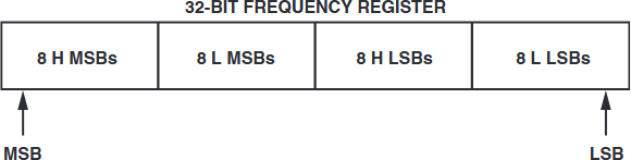
The AD9832 contains a 32-bit frequency register. The register is shown below and is broken up into four bytes. Since the AD9832 accepts only eight bits of data in any one command, in order to fully program the 32-bit register the user must input four commands, each delivering only eight bits of data.
For addressing purposes, the 32-bit register is broken up as follows: The 16 MSBs are defined as having eight higher bits (H) and eight lower bits (L). Similarly, the 16 LSBs have the same addressing scheme, eight higher (H) bits and eight lower (L) bits.

The Frequency Word
The frequency word is the 32-bit word which the user inputs into the frequency register. This determines the output frequency and is based on the ratio of the required output frequency to the reference clock frequency. In the example below, the reference clock is 25 MHz. The required output needs to be 5 MHz, so the frequency word is calculated as:
(5/25) × (0xFFFFFFFF) = 0x33333333
The Defer Register
The defer register (16 bits wide) acts as a buffer register to the last register written to. The defer register is written to in two writes. The first eight bits will be held (deferred) in the register until the next eight bits are written in. When all 16 bits have been written into the defer register, the frequency register will be updated. The defer register always points to the last address that was written to.


Since the defer register has stored the last 16 bits written to it and is still pointing to the frequency register previously addressed, it is possible to update either the lower eight bits or the upper eight bits of that frequency register with one write. This is called a direct write and is actually the last part of a normal write sequence.
Note that if users want to write to any other register, they will have to do a full write sequence as shown above.
Entire Command Sequence for 5 MHz Program
0xF800 Binary (1111 1000 0000 0000)
0x3333 Binary (0011 0011 0011 0011)
0x2233 Binary (0010 0010 0011 0011)
0x3133 Binary (0011 0001 0011 0011)
0x2033 Binary (0010 0000 0011 0011)
0xC000 Binary (1100 0000 0000 0000)
Command Sequence Explained
For the purpose of this explanation, the 16-bit SPI word will be addressed as follows:
D15, D14, D13, ..., D2, D1, D0
| 0xF800 | Binary (1111 1000 0000 0000) |
| D15, D14 | 1,1. This means that bits D13, D12, and D11 are active. In this case: |
| D13 | 1, SLEEP bit. This puts the part into sleep mode. |
| D12 | 1, RESET bit. This sets the part into reset, i.e., output of the DAC will be midscale. |
| D11 | 1, CLR bit. When CLR = 1, SYNC and SELSRC are set to 1. This sets control of choosing which register is selected to external pins, not through software. CLR will automatically reset to 0. |
| D10...D0 | 0. (These are Don’t Care bits, X.) |
| The part is now ready to be programmed. | |
| 0x3333 | Binary (0011 0011 0011 0011) |
| Command broken down as follows: | |
| 0011 | /* Write to Frequency 0 Reg, H MSBs */ |
| 0011 | /* Write to Frequency 0 Reg, H MSBs */ |
| 0011 0011 | /* Eight bits of data to write */ |
| 0x2233 | Binary (0010 0010 0011 0011) |
| 0010 | /* Write eight frequency bits to defer register */ |
| 0010 | /* Write to Frequency 0 Reg, L MSBs */ |
| 0011 0011 | /* Eight bits of data to write */ |
| 16 bits are now loaded to the upper 16 bits of Frequency Register 0. | |
| 0x3133 | Binary (0011 0001 0011 0011) |
| 0011 | /* Write eight frequency bits to defer register */ |
| 0001 | /* Write to Frequency 0 Reg, H LSBs */ |
| 0011 0011 | /* Eight bits of data to write */ |
| 0x2033 | Binary (0010 0000 0011 0011) |
| 0010 | /* Write eight frequency bits to defer register */ |
| 0000 | /* Write to Frequency 0 Reg, L LSBs */ |
| 0011 0011 | /* Eight bits of data to write */ |
| 16 bits are now loaded to the lower 16 bits of Frequency Register 0. | |
| 0xC000 | Binary (1100 0000 0000 0000) |
| D15, D14 | 1,1. This means that bits D13, D12, and D11 are active. In this case: |
| D13 | 0, SLEEP bit. Takes the part out of sleep mode. |
| D12 | 0, RESET bit. Takes the part out of reset mode. |
| D11 | 0, CLR bit. |
| D10...D0 | 0 (Don’t Care bits for this command.) |
5 MHz will now appear on the output pin. The FSELECT pin must be pulled to GND to choose Frequency Reg 0.
Author
