AN-2563: Thermocouple Temperature Measurement System with Less Than 500 μA Current Drain
Circuit Function and Benefits
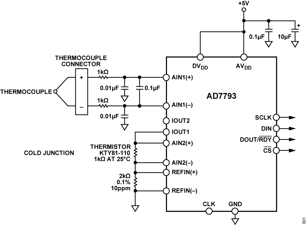
The circuit shown in Figure 1 is a complete thermocouple system based on the AD7793 24-bit sigma-delta (Σ-Δ) analog-to-digital converter (ADC). The AD7793 is a low power, low noise, complete analog front end for high precision measurement applications. The device includes a programmable gain amplifier (PGA), an internal reference, an internal clock, and excitation currents, thereby greatly simplifying the thermocouple system design.

The AD7793 consumes only 500 µA maximum, making it suitable for any low power application, such as smart transmitters where the complete transmitter must consume less than 4 mA. The AD7793 has a power-down option. In this mode, the complete ADC, along with its auxiliary functions, is powered down so that the part consumes 1 µA maximum.
Because the AD7793 provides an integrated solution for thermocouple design, it interfaces directly to the thermocouple. For the cold junction compensation, a thermistor along with a precision resistor is used. These are the only external components required for the cold junction measurement other than some simple RC filters for electromagnetic compatibility (EMC) considerations.
Circuit Description
A Type T thermocouple is used in the circuit. This thermocouple (made from copper and constantan) measures temperature from −200°C to +400°C. It generates a typical temperature dependent voltage of 40 µV/°C.
The thermocouple response is approximately linear over a small portion of its entire temperature range, from 0°C to 60°C (see Figure 2).


Cold Junction Compensation
Thermocouples measure the temperature difference between two points, not an absolute temperature. To measure a single temperature, maintain one of the junctions (normally the cold junction) at a known reference temperature, and the other junction at the temperature to be sensed.
Having a junction of known temperature is not convenient for most applications; therefore, a thermally sensitive device is placed on the printed circuit board (PCB). This thermistor is used to measure the temperature of the thermocouple input connection. The thermistor fits inside the metallic tab found on the thermocouple connection, minimizing any temperature gradients that may exist.
Because the voltage from a known cold junction is simulated, the appropriate correction can be applied. See the Thermocouple Linearization section for more detailed information on processing and manipulating the thermocouple and thermistor voltages to produce an accurate temperature reading.
ADC Channel 1 Configuration, Thermocouple
The temperature range for the thermocouple is −200°C to +400°C. The typical temperature dependent voltage generated by the thermocouple is 40 µV/°C. This voltage generates a thermocouple voltage range of −8 mV to +16 mV.
When reading the thermocouple voltage, the ADC uses the external 2 V reference and is configured for a gain of 64. This defines the analog input voltage range as ±31.25 mV (±VREF/Gain). For a gain of 64, the absolute voltage on the analog inputs must be between GND + 300 mV and AVDD − 1.1 V.
Because the AD7793 operates from a single power supply, the signal generated by the thermocouple must be biased above ground so that it is within the acceptable range of the ADC. The bias voltage generator on-board the AD7793 biases the thermocouple signal so that it has a common-mode voltage of AVDD/2.
ADC Channel 2 Configuration, Thermistor
The second channel of the ADC monitors the voltage generated across a thermistor being driven by one of the current output pins of the AD7793. A 1mA excitation current drives the series pair of thermistor and precision resistor (2 kΩ, 0.1%), as shown in Figure 1.
The thermistor value varies from 0°C (815 Ω) to 30°C (1040 Ω), producing a voltage signal range of 815 mV to 1040 mV. The precision resistor produces 2.0 V for use as an external reference. With a gain of 1, the analog input range is ±2 V (±VREF/Gain). This architecture gives a ratiometric configuration. Any change in the value of the excitation current does not alter the accuracy of the system.
Assuming a linear transfer function between 0°C and 30°C, the relationship between the cold junction temperature and the thermistor resistance, R, is:

One other consideration is the output compliance of the IOUT1 pin of the AD7793. When the 1 mA excitation current is used, the output compliance equals AVDD − 1.1 V. This specification is met because the maximum voltage at IOUT1 equals the voltage across the precision resistor plus the voltage across the thermistor, which equals 2 V + 1.04 V = 3.04 V.
Output Coding
The output code for an input voltage on either channel is:

Where:
AIN is the analog input voltage.
GAIN is the in-amp setting.
N = 24.
Thermocouple Linearization
As mentioned in the Circuit Description section, the thermocouple is only approximately linear over a small temperature range. In fact, the thermocouple is highly nonlinear over the rest of the temperature range.
The National Institute of Standards and Technology provides ITS-90 look-up tables for thermocouples. Each table contains a list of thermoelectric voltages (mV) and their corresponding temperatures.
To implement the cold junction compensation previously mentioned, consult the Type T thermocouple look-up table and search for the thermoelectric voltage associated with the cold junction temperature. Then, subtract this thermoelectric voltage from every element in the look-up table to produce a cold junction compensated thermoelectric voltage look-up table.
System Noise Considerations
For an output data rate of 16.7 Hz and a gain of 64, the rms noise of the AD7793 equals 0.086 µV (noise is referred to input). The peak-to-peak noise is:

If the thermocouple has a sensitivity of precisely 40 µV/°C, the thermocouple should measure the temperature to a resolution of:
0.5676 µV ÷ 40 µV = 0.014°C
Test Data and Results
A CL540ZA source (and appropriate Type T cable) was used to simulate the thermo-couple input. The CL540ZA is capable of simulating several different types of thermocouples (J, T, E, K, R, S, B, N, and so on).
According to Figure 3, the error over the entire temperature range is less than 1°C. However, over most of the range, the error is less than 0.5°C.


The peak-to-peak noise of the AD7793 was determined by shorting the input pins of the ADC together and acquiring 1000 samples. As seen in the histogram found in Figure 4, the code spread is approximately 220 codes, which translates to a temperature spread of 0.02°C peak-to-peak.


Common Variations
The AD7793 is a low noise, low power ADC. Other suitable ADCs are the AD7792 and AD7785. Both parts have the same feature set as the AD7793. However, the AD7792 is a 16-bit ADC while the AD7785 is a 20-bit ADC.