AN-1344: High Common-Mode Voltage Current Loop Transmitter Front End
Introduction
The current loop is a common signaling technique for sending and receiving sensor data over long distances. In a currentloop, the current contains information from a transmitter that is relayed to a receiver through very long wires (see Figure 1). This transmission technique has an inherent insensitivity to electrical noise, thus making it ideal for data transmission. Unlike voltage signaling, current loops are immune to errors induced by IR drops along the wires. Although the wire terminations in a loop are less than ideal, allsignaling currents flow through all components. IR drops do not affect the signaling current as long as the supply is greater than the combined voltage drop around the loop.

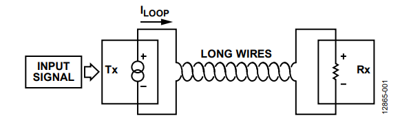
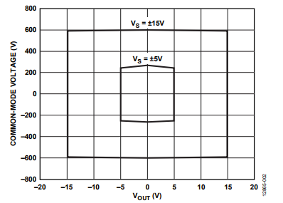
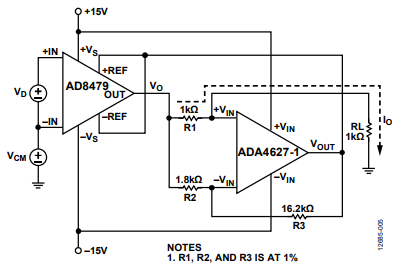
This application note highlights the AD8479, a precision difference amplifier that accurately measures differential signals with the presence of very high input common-mode voltages (CMVs) that range up to ±600 V (see Figure 2). The AD8479 serves as a front end for a current loop transmitter, thus enabling the transmitter to operate in applications with very high CMV, such as motor controls and high voltage current sensing.

Circuit Transfer Function
Even at very high CMV, the AD8479 accepts differential voltage and passes it through its output with a fixed gain of 1 and the transfer function given by Equation 1.

where:
VO is the AD8479 output shown in Figure 3.
VD is the AD8479 differential input voltage shown in Figure 3.
VREF is the voltage applied to the +REF and –REF pins.

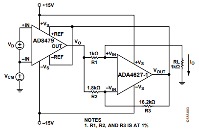
Because the +REF and –REF pins are tied, the output is equal to the reference voltage (VREF) when there is no differential voltage present at the input.
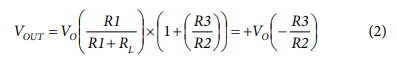
The output goes to the ADA4627-1, which serves as an interface between the AD8479 and the load. Connecting the output to the ADA4627-1, as opposed to connecting it directly to the AD8479 output, helps to avoid variations on the output current, which is highly affected by the load change. The ADA4627-1 also forces the voltage for the reference pins of the AD8479, resulting in the following output equation:
Combining the AD8479 and ADA4627-1 enables a current loop transmitter front-end circuit to measure signals at very high CMVs.
From Equation 2 and the values shown in Figure 3,
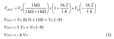
From Equation 1, the following is true:
VO = VD + VREF
where VREF = VOUT.
Therefore,
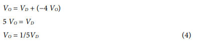

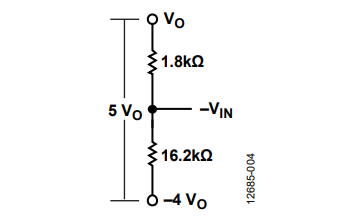
Use the voltage divider theorem to calculate the following:
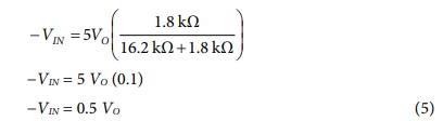
With the virtual short, calculate the following:
–VIN = +VIN
+VIN = 0.5 VO
Therefore,
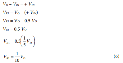
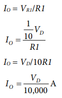
Figure 5 shows the current path that carries the information. Because the amplifier (ADA4627-1) has high input impedance, the current flows directly through the load, which gives an overall circuit transfer function of.

Current Loop Transmitter Accuracy
Approximate the total error contributed by the resistor tolerances by assuming that each of the critical resistors contributes equally to the total error. The three critical resistors are R1, R2, and R3. Resistors with a worst-case tolerance buildup of 1% yield a total resistance error of 3% maximum. If root sum square (RSS) errors are assumed, the total RSS error is 1√3 = 1.732%.
| Error Component | Error | Error Value | Total Uncompensated Error (%FSR) |
| AD8479 | Offset | 3 mV | 0.03% |
| AD8479 | Gain | 0.02% | 0.02% |
| Maximum Full-Scale Error | 0.05% |
Adding the worst-case resistor tolerance error of 3% to the worst-case errors due to the offsets of active components yields:
Full Scale Error = 3% + 0.05% = 3.05%
These errors assume that the ideal resistors were selected and that the errors resulted from their tolerances. Figure 6 shows the actual error performance of the application circuit.

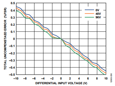
For a maximum uncompensated error of 0.47% FSR, the system shows highly dependable performance in terms of accuracy. Despite the errors introduced by the resistors and the AD8479, the system is able to maintain good accuracy over different CMV values. With this performance, using the AD8479 as a current loop transmitter front end enables instrumentation with high accuracy up to 96 V (guaranteed to work up to ±600 V CMV). Because the majority of the errors are introduced by passive components, system performance can be improved further by using high precision, very tight tolerance resistors.

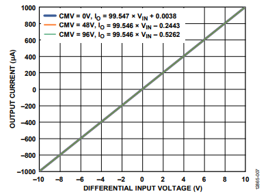
Figure 7 shows the transmitter output performance at three CMVs. At 0 V CMV, a 45.3 ppm gain error with an offset of 0.0038 μA is present; at 48 V CMV, a 45.4 ppm gain error with an offset of −0.2443 μA is present; and at 96 V CMV, a 45.4 ppm gain error with an offset of −0.5262 μA is present. This performance characteristic demonstrates that increasing the CMV has a negligible effect on the output of the transmitter front end. This result is due to the AD8479 allowing accurate measurement of differential signals in the presence of CMV up to ±600 V due to the ADA4627-1, a very low offset voltage wide bandwidth precision amplifier.
In addition, this application circuit has an excellent commonmode ratio (CMR) of 94 dB in both 0 V and 48 V CMVs and 48 V and 96 V CMVs as measured.
Conclusion
Current loop signaling is more dependable than voltage signaling for transmitting signals over long distances. Signals are contained in the loop current transmitted for long distances, disregarding the effects of voltage drops in the wire, a major concern for voltage signaling. When transmitting signals as voltage, the supply current induces voltage drops along the wires that usually appear as errors in the signal measurement. Furthermore, current loop signaling has a better immunity to noise than voltage signaling. This application note implements a current loop transmitter front end using the AD8479. This allows precision instrumentation over very high CMV signals. This circuit addresses the need for precision measurements for industrial and motor applications, that is, industrial process-monitoring applications. As tested and verified, this application circuit allows precision instrumentation at CMVs up to 96 V (works up to 600 V CMV) with proven accuracy over wide input voltage and CMV ranges. The Analog Devices, Inc., amplifier devices used in this application note are highly dependable for robust and precision application needs.
Authors

