AN-1085: Multiplying DACs—AC/Arbitrary Reference Applications
Introduction
A multiplying digital-to-analog converter (DAC) differs from the conventional fixed reference DAC by having the ability to operate with an arbitrary or ac reference signal. This application note details the basic theory behind current output multiplying DACs, and why these DACs are so suitable for ac voltage and arbitrary voltage conditioning.
Basic Waveform Attenuation
A simple method of adjusting the gain of an ac signal is to use the classic inverter op amp stage, choose an amplifier with sufficient bandwidth, and adjust the gain by using the following equation:
VOUT = −[RDAC/RFB(VIN)]
Multiplying DACs offer an ideal building block for multiplying an arbitrary or ac voltage signal. The buffered current output DAC architecture is based on a noninverting gain amplifier structure. A multiplying DAC uses an R-2R architecture to replicate the functionality of the variable RDAC resistor shown in Figure 1. The input impedance to the DAC seen at the VREF pin is fixed, and the output impedance is code dependent to give the equivalent variable RDAC value.
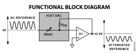
Figure 1. Inverting Gain Configuration.
The terms AD55xx and AD54xx used in this application note reference the multiplying DACS listed on www.analog.com/MultiplyingDAC.
Multiplying DACS
In a multiplying DAC, current is steered to either the virtual ground connected to the IOUT1 node or the ground node (in some parts this is the IOUT2 node), which allows for a very low glitch output voltage (see Figure 2).
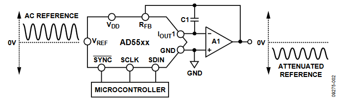
Figure 2. Multiplying DAC, VOUT = 0 V to −VREF.
One of the key advantages in using an IOUT DAC in this configuration is that the integrated RFB resistor is matched to the RDAC equivalent resistor allowing for very low gain temperature coefficient errors.
When an output amplifier is connected in unipolar mode, as shown in Figure 2, the output voltage is given by:
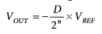
where:
D is the fractional representation of the digital word loaded to the DAC.
D = 0 to 255 (8-bit AD5450).
= 0 to 1023 (10-bit AD5451).
= 0 to 4095 (12-bit AD5452).
= 0 to 16,383 (14-bit AD5453).
= 0 to 65,536 (16-bit AD5543).
n is the number of bits.
In brief, the output signal of a multiplying DAC is proportional to the product of the reference input and the digital input number.
Adding Gain
In applications where the output voltage must be greater than VIN, gain can be added with an additional external amplifier, or it can be achieved in a single stage.
Increase the gain of the circuit by using the recommended configuration shown in Figure 3. R1, R2, and R3 should have similar temperature coefficients, but they must not match the temperature coefficients of the DAC.
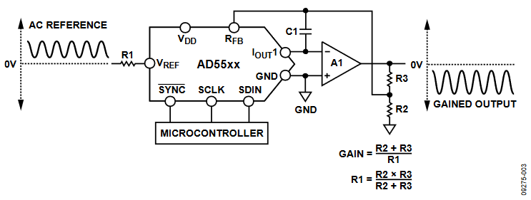
Figure 3. Signal Gain Using Multiplying DACs.
Positive Voltage in/positive Voltage Out
To generate a positive voltage output from a multiplying DAC configuration, an extra inverting amplifier can be added to the signal chain to reinvert the output. Another option is to select a part with uncommitted resistors, as shown in Figure 4. The advantage with uncommitted resistors is that they have very similar temperature coefficients.
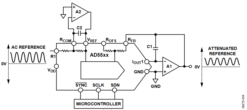
Figure 4. Multiplying DAC, VOUT = 0 V to VREF.
Single-ended-to-differential Configuration
To generate a differential output from this configuration, two extra op amps are required. See the CN-0143 Circuit Note, Single-Ended-to-Differential Converters for Voltage Output and Current Output DACs Using the AD8042 Op Amp, for detailed information on this.
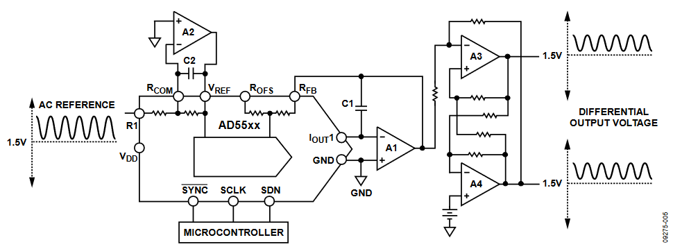
Figure 5. Single-Ended-to-Differential Configuration.
Stability Issues
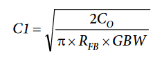
An important component to take into account in achieving the desired waveform conditioning signal is the compensation capacitor. The internal output capacitance of the DAC introduces a pole into the open-loop response that can cause ringing or instability in the closed-loop ramp profiling circuit. To compensate for this, an external feedback capacitor, C1, is usually connected in parallel with the internal RFB of the DAC (see Figure 2). If the value of C1 is too small, it can produce waveform distortion at the output, and if the value of C1 is too large, it can adversely affect the bandwidth of the system. Because the internal output capacitance of the DAC varies with code, it is difficult to fix a precise value for C1. The value is best approximated according to the following equation:
where:
GBW is the small signal unity-gain bandwidth product of the op amp in use.
CO is the output capacitance of the DAC.
Key DAC Specifications for Signal Conditioning
Some of the key selected ac specifications that must be taken into account when multiplying an ac/arbitrary reference input signal include multiplying bandwidth, analog total harmonic distortion, and multiplying feedthrough error.
Multiplying Bandwidth
The multiplying bandwidth is the reference input frequency at which the gain is −3 dB. For a given device, it is a function of amplitude and the choice of compensation capacitance. Figure 6 shows multiplying bandwidth plots for the AD5544, AD5554, or AD545x current output DACs, which can multiply signals up to 12 MHz. The 350 MHz bandwidth of the accompanying low power AD8038 op amp insures that the op amp introduces insignificant dynamic errors on this scale.

Figure 6. Multiplying Bandwidth.
Analog Total Harmonic Distortion
Analog total harmonic distortion is a mathematical representation of the harmonic content in the multiplied waveform signal. It is the rms sum of the harmonics (V2, V3, V4, and V5) of the DAC output to the fundamental value, V1, given by:
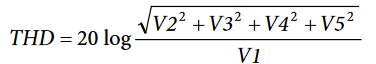
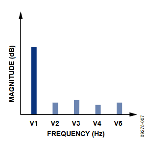
Figure 7. Total Harmonic Distortion.
Multiplying Feedthrough Error
The multiplying feedthrough error is defined as the error due to capacitive feedthrough from the reference input to the DAC output when all 0s are loaded to the DAC. Ideally, every time a bit drops 6 dB loss incurs in the gain extending to DB0 (see Figure 8). However, for lower bits, the multiplying feedthrough affects the gain of the part. This is shown in Figure 8 by the flat lines tailing upward for the lower bits. For example, at DB2 for a 14-bit DAC at 1 MHz, it should be 72 dB; however, because of feedthrough, it is actually 66 dB.
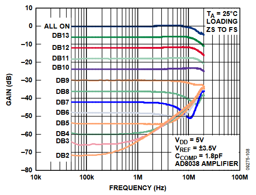
Figure 8. Multiplying Feedthrough Error.
Choosing the Correct Op Amp
Multiplying DAC circuit performance is strongly dependent on the ability of the selected op amp to maintain the voltage null at the ladder output and perform the current-to-voltage conversion. For best dc accuracy, it is important to select an operational amplifier with low offset voltage and bias current to keep errors commensurate with the resolution of the DAC. Detailed op amp specifications are included in device data sheets.
For applications where the reference input is a relatively high speed signal, a wide bandwidth, high slew rate op amp is required to avoid degrading the signal. The gain bandwidth (GBW) of an op amp circuit is limited by the impedance level of the feedback network and the gain configuration. To determine what GBW is required, a useful guideline is to select an op amp with a −3 dB bandwidth that is 10 times the frequency of the reference signal.
The slew rate specification of the op amp must be considered to limit distortion of large high frequency signals. For the AD54xx and AD55xx families, an op amp with a slew rate of 100 V/µs is generally sufficient.
Table 1 provides a selection of operational amplifiers that are useful for multiplying applications.
For additional information, see the multiplying DAC product page at www.analog.com/MultiplyingDAC.
| Part No. | Supply Voltage (V) | BW @ ACL (MHz) | Slew Rate (V/µs) | VOS (Maximum) (µV) | IB (Max) (nA) | Packages |
| AD8065 | 5 to 24 | 145 | 180 | 1500 | 0.006 | SOIC-8, SOT-23-5 |
| AD8066 | 5 to 24 | 145 | 180 | 1500 | 0.006 | SOIC-8, MSOP-8 |
| AD8021 | 5 to 24 | 490 | 120 | 1000 | 10,500 | SOIC-8, MSOP-8 |
| AD8038 | 3 to 12 | 350 | 425 | 3000 | 750 | SOIC-8, SC70-5, SOT-23-5 |
| ADA4899-1 | 5 to 12 | 600 | 310 | 35 | 100 | LFCSP-8, SOIC-8 |
| AD8057 | 3 to 12 | 325 | 850 | 5000 | 500 | SOT-23-5, SOIC-8 |
| AD8058 | 3 to 12 | 325 | 850 | 5000 | 500 | SOIC-8, MSOP-8 |
| AD8061 | 2.7 to 8 | 320 | 650 | 6000 | 350 | SOT-23-5, SOIC-8 |
| AD8062 | 2.7 to 8 | 320 | 650 | 6000 | 350 | SOIC-8, MSOP-8 |
| AD9631 | ±3 to ±6 | 320 | 1300 | 10,000 | 7000 | SOIC-8, PDIP-8 |
Author
