78M6610+LMU In-System Calibration
Abstract
This document describes the 78M6610+LMU configuration, including scaling, input setup, and in-system calibration procedures. The 78M6610+LMU data sheet and the 78M6610+LMU Evaluation Kit User Manual are helpful references for understanding the contents of this document.
Introduction
To report accurate measurement results, some level of calibration is needed. For system accuracy requirements of a few percent, a fixed set of calibration coefficients to match the nominal gain values for a given bill of materials can be used. When requirements dictate better system accuracy than component tolerances allow, each system must go through its own calibration routine during the manufacturing process. This document walks the user through the initial configuration and calibration of the 78M6610+LMU energy measurement processor (EMP). Topics covered include:
- Calibration parameters
- Scaling factors
- Calibration setup considerations
- Examples using the evaluation kit
A data sheet and evaluation kit user manual for the 78M6610+LMU are helpful references for understanding the contents of this document.
Calibration Parameters
A typical integrated circuit designed for energy metering applications is often temperature compensated and contributes less than 0.2% error to the system's measurement accuracy. A number of calibration parameters are needed to compensate for non-ideal (off-chip) components in the sense circuit. Figure 1 shows a simplified signal path with all the parameters included with Maxim's energy measurement processors. This section explores each parameter and their recommended usage.

Figure 1. Simplified signal path for EMPs.
*Parameter with Integrated calibration routine for determining correct value
Calibration Routines
The 78M6610+LMU provides integrated calibration routines for quickly determining the correct calibration values for die temperature, voltage, and current. A single-point calibration is often adequate to calculate the correct system gain settings. The newly calculated gains can be stored in the on-chip flash memory as new defaults.
Alternatively, the user can determine these values with an external routine (for per unit calibration values) or from statistical analysis (for fixed-to-BOM) calibration values. These options are not covered in this application note.
Input Configuration Requirements
The 78M6610+LMU allows dynamic configuration of the analog inputs to accommodate several sensor topologies and system configurations. Regardless of the configuration selected for normal operation, all gain calibration routines must be executed in a configuration with a 1:1 relationship between a sense input and the respective low-rate RMS output (and target value).
Offset Removal (HPF Block)
For sinusoidal AC voltages and currents, dynamic offset removal using the highpass filter (HPF) block is recommended. This is accomplished with either lump-sum removal or a more gradual averaged reduction. The latter is similar to highpass filtering, but without phase distortion. All methods are controlled by the HPF coefficient registers and do not involve calibration.
For load currents with a DC component, such as a half-wave rectifier feeding a load, the dynamic offset removal must be disabled. Setting HPF coefficients equal to zero effectively stops dynamic updates of the offset registers. The user can then perform an offset calibration and save offset values as defaults (along with HPF coefficients).
Phase Offsets
Phase errors caused by sensors and board-level components can introduce error in the reported power measurements (RMS voltage and current measurements are unaffected by phase). When using resistive sensors for both current and voltage, a negligible offset is introduced by component variations in the off-chip RC filter. When using current or voltage transformers for sensing, however, a significant phase shift may be introduced. Fortunately, using a nominal value for a fixed set of transformers is acceptable for most designs.
Fortunately, using a nominal value for each system is acceptable as phase offset is constant for most sensors. Per unit calibration is only necessary when the accuracy of power measurements must be maintained at low power factors. (See Figure 2.) The following equation represents the error in power measurements (for sinusoidal loads) as a function of the CT phase shift (α) and the cos(θ) (PF).
Error = 1 - (cos(θ + α)/cos(θ))

Figure 2. Power Measurement Error vs. Power Factor.
To determine phase shift (a) between the current-sense path and voltage-sense path, reference equipment with sinusoidal waveforms can be set to an expected angle in the 30° to 60° range and collect active power (P) and apparent power (S) measurements.

Φ = cos-1(P/S) = tan-1(Q/P) = sin-1(Q/S)
phase compensation in radians = α = expected angle - -1
phase compensation in samples = (α/2π) × (sample rate/line frequency)
The value to be entered in the phase compensation register needs to be converted to a S.21 register type:
PHASECOMP = (phase compensation in samples) × 221
RMS and Power Offsets
These offsets are applied at the end of accumulation intervals to adjust the RMS and power measurement results. The error associated with these parameters can generally be attributed to wideband noise introduced through layout traces, ADC sample dithering, and minor computational rounding errors. Unless the user has a highly variable current noise floor, this parameter should be set based upon the historical statistical values.
Assuming all other parameters are accurately calibrated or have insignificant effect upon error, the recommended IRMS offset parameter value can be calculated using a single calibration point as follows.
IRMSREF << Full-Scale Current
IRMS_OFFSNEW = IRMS_OFFSOLD + (IRMS(REF2-, IRMSMEA2)/IRMS_OFFSLSB)
The calibration adjusts the offset for the active power. It is recommended that the user set this parameter based upon the historical statistical values for a given system design.
Assuming all other parameters are accurately calibrated or have insignificant effect upon error, the recommended power offset parameter value can be calculated using a single calibration point as follows.
PREF << Full-Scale Power
P_OFFSNEW = P_OFFSOLD + ((P(REF - PMEA))/P_OFFSLSB)
…
Nonvolatile Storage
Whether manually setting the calibration parameters or using the integrated routines, the host must issue a command to save the calibration parameters to flash as defaults. A single command saves the present value of any register designated as nonvolatile in the respective data sheet.
Scaling Factors
The hardware for any design determines the voltage and current ranges that can be measured. Sensors effectively scale AC voltages down to measurable voltages and convert currents to measurable voltages. Registers corresponding to measurement values are in raw format and must be scaled by the user to properly read (or write) the intended values. The simplest method for determining scaling factors assumes a linear system response across the entire measurable range. Alternatively, users can stretch or compress the scaling factor to trade range for resolution.
Note: The same scaling factors used to determine calibration parameters must also be used for reading back measurements. The first step in configuring and calibrating a measurement device is to define the scaling factors for translating real world reference values into calibration targets (and subsequently measurements into real world values). The 78M6610+LMU solution provides nonvolatile scratchpad registers for storing information about scaling factors needed for making sense of register information.
Register Format
All measurement registers are stored as 24-bit two's complement values. This gives the registers' raw value (Rr) a theoretical range of 223-1 (0x7FFFFF) to -223 (0x800000). These registers are expressed, by convention, with the notation of S.23, which implies the interpreted value of the register (Ri) is the raw value (Rr) divided by 223. This gives the registers an interpreted range of +1.0 - 1/223 (0x7FFFFF) to -1.0 (0x800000).
Ri = Rr/223
Full-Scale Values
To get real world measurement from a register, the user must apply a scaling factor to the interpreted value. The real world value (Rv) is the interpreted value (Ri) multiplied by the corresponding full-scale value (FSx). Three distinct full-scale values are recommended: FSV for voltage (RMS and peak), FSI for current (RMS and peak), and FSP for power (inclusive of active, reactive, and apparent). The LSB of the register is then the full-scale value (FSx) divided by 223.
LSBR = FSx/223
Rv = Ri × FSx = Rr × LSBR = Rr/223 × FSx
Choosing and consistent use of proper full-scale values (FSx) is important for extracting the real world measurements from the device. The full-scale values (FSx) are intended to represent the sensors' scaling of real world values (volts and amps) into the ADC inputs (±250mVpk).
For all power measurements, full-scale power (FSP) is always equal to the product of FSI and FSV:
FSP = FSI × FSV
Ideal Full Scale
The ideal full-scale value (FSxideal) is the input value that ideally generates 250mVpk on the ADC input. This value assumes the device is perfectly trimmed and uncalibrated and has ideal component values. A typical evaluation board has a voltage-divider for line voltage measurement (Figure 3) consisting of two 1MΩ resistors in series with a 750Ω resistor, as shown below.

Figure 3. Typical evaluation board for line voltage measurement.
The line voltage is applied across the entire resistor chain, and the ADC input is the voltage across the 750Ω resistor. The voltage at the input to the ADC, VADC, can be calculated as:
VADC = VLINE × (750/(750 + 2 × 10Ω6))
This scales the input line voltage by a factor of 2667.666. The ADC can measure ±250mVpk so, with this voltage-divider, the maximum voltage that can be measured by the device is:
FSVideal = (±0.250Vpk)/((750/(750 + 2 × 10Ω6))) ≅ ±666.917Vpk
User Full Scale
The user can choose to use a full-scale value (FSx) that is different from the ideal value (FSxideal) for a variety of reasons including, but not limited to, non-uniform sensor topologies, storage limitations, and/or ease of measurement data conversion. The user should choose one full-scale value for all outputs associated with a measurement type (voltage, current, or power).
While the user may choose to use a full-scale value (FSx) that is different from the ideal value (FSxideal), there are some limitations on the viable choices and each choice has some implications for performance. When choosing an FSx different from the ideal, it is assumed that the device will adjust the gain parameters during calibration to accommodate that value.
All gain parameters are stored as 24-bit two's complement values. This gives the register's raw gain value (Gr) a theoretical range of 223 - 1 (0x7FFFFF) to -223 (0x800000). These registers are expressed, by convention, with the notation of S.21, which implies the interpreted value of the register (Gi) is the raw value (Gr) divided by 221. With negative numbers being invalid, this gives the registers an interpreted range of +4.0 - 1/221 (0x7FFFFF) to 0. The raw default (0x200000) is interpreted as +1.0.
Gi = Gr/221
FSx < FSxideal
Choosing an FSx for scaling below the ideal value (FSxideal) forces the device to increase the gain on that slot to compensate. The gain (Gi) is limited to approximately +4.0 so the user should never choose an FSx that is significantly larger than any ideal value FSxideal.
FSx > FSxideal
Choosing an FSx for scaling above the ideal value (FSxideal) forces the device to decrease the gain on that slot to compensate. A smaller gain (Gi) can eventually reduce the granularity of the gain compensation and LSB of the measurement registers. The gain register is an S.21 giving it 21 significant bits of granularity below +1.0 (0x200000). With 10 bits giving approximately 0.1% granularity (1/210 = approximately 0.00098) the gain register has another 11 bits to work with. This is sufficient for most systems, but special care must be taken to ensure the LSB of the power registers does not get too large.
Nonvolatile Storage of FSx
As previously noted, it is important that the same full-scale values (FSx) used for setup and calibration be used for subsequent measurements. The host or user must therefore have some way to store these values for later use. This can be done off-chip or with the integrated nonvolatile internal storage. The usage of these nonvolatile registers is user defined and their content has no effect on the internal operations of the device.
Example

Figure 4. Example of two sensors.
In the example above (Figure 4) with two sensors:
A CT used on line current IB with a 2500:1 primary-to-secondary turn ratio is paired with a 1Ω burden resistor. Therefore the maximum primary current that can be applied is:
FSIIDEAL = (±0.250Vpk)/(1Ω) × 2500 ≅ ±625 APK
A 0.004Ω shunt resistor used on neutral current IN. Therefore the maximum current that can be applied is:
FSIIDEAL = (±0.250Vpk)/(0.004Ω) = ±62.5APK
In this scenario IB and IN need to be combined mathematically (IA = IN - IB) to produce IA for measurement. The LSB (and therefore FSI) of two readings must be the same to allow for this function. Since the ideal full-scale values (FSIideal) do not match we must choose a value that can accommodate both sensor topologies and let the calibration functions adjust the gains to match.
If the user chooses an FSI of 62.5Apk (to match a 0.004Ω shunt perhaps) any attempt to calibrate this current input results in a gain overflow (attempts to program Gi = approximately 10) and calibration fails. It is recommended to choose the larger of the two values (±625APK) as the basis for the FSI to allow the gain(s) the most room to compensate.
The host can assume the use of VFSCALE to store the full-scale voltage (FSV) and IFSCALE to store the full-scale current (FSI) as integers. FSP is derived as FSV × FSI. So if VFSCALE contains 667 (0x00029B) and IFSCALE contains 625 (0x000271) then FSV is 667V, FSI is 625A, and FSP is 416875W. Notice in this scenario that the LSB of the power variables is almost 50mW.
| RMS Voltage(A) = VA_RMS/223 × 667 |
RMS Current(A) = IA_RMS/223 × 625 |
Watts(A) = WATT_A/223 × 416875 |
| LSBVA_RMS = 667/223 = 0.0000795 volts |
LSBIA_RMS = 625/223 = 0.0000745 amps |
LSBWATT_A = 416875/223 = 0.0496954 watts |
Calibration
To properly calibrate the gain coefficients for voltage and current channels, a stable reference AC signal and a stable load must be applied to the channels for calibration. It is important to make sure the reference equipment is also placed on the same side of the power supply as the measurement circuit as shown in Figure 5.

Figure 5. Reference equipment placed on the same side of the power supply.
Calibrating On-Chip Temperature Sensor
It is possible to recalibrate the on-chip temperature sensor (offset) applied by the factory automated test equipment (ATE). To calibrate the sensor, a known temperature must be entered to the T_TARGET register. The target temperature to be entered is the ambient temperature measured in proximity of the device.
The user initiates the Temperature Calibration Command in the Command Register (not combined with any other calibration commands). This updates the T_OFFS offset parameter with a new offset based on the known temperature supplied by the user. The T_GAIN gain register is set by the factory and not updated with this routine. The range of the Die Temperature registers is -128 to +128 - LSB°C.
Inputs (Slots) Configuration
The 78M6610+LMU solution offers flexibility for configuring the calculation of RMS current as a combination of the input slots S1and S3 as shown in Figure 6.

Figure 6. Combination of input slots for configuring RMS.
In the example presented in the Example section, the neutral current sensor is connected to input S1 and the CT is connected to input S3. For calibration setup, IA should be defined as S1 to maintain a 1:1 sensor to input mapping during calibration.
Note that in a split-phase system with a balanced load, the current in the neutral is, in theory, zero (refer to the data sheet for details). To provide a non-zero signal to the neutral sensor, a simple solution is to set the current in phase A to zero by either opening the load or by using a programmable load.
Current and Voltage Target Setup
The RMS value corresponding to the applied reference voltage Vrefrms must be entered in the relevant target register (VTARGET, ITARGET). The target value to enter is calculated as follows:
VTARGET = Vrefrms/VFSCALE
where VFSCALE is the full-scale value of the input voltage channel.
Similarly for the current:
ITARGET = Irefrms/IFSCALE
where Irefrms is the RMS value of the current applied to the input channel for calibration and IFSCALE is the full-scale value of the input current channel as explained in the Scaling Factors section.
Calibration Command
The Command register is used to start a calibration sequence through the calibration command. The calibration command allows the selection of the inputs to be calibrated and to start the calibration process.
Prior to initiating a calibration command, the slot configuration (CONFIG register) should be such that the voltage and current results are those of the sensor that is being calibrated. As such, the current configuration bits should be set as: IA = S1; IB = S3 to calibrate the current channels (slots S1 and S3). Analogously, for voltage channels, the configuration bits should be VA = S0; VB = S2 during calibration.
Note that multiple voltage and current channels can be calibrated simultaneously. The only limitation is that, due to the single ITARGET register (used for current slots 3 and 1) and VTARGET register (used for voltage slots 0 and 2), the same target voltage or current must be applied to all phases. Considering calibration is done with RMS results, the value of the target register should never be set to a value above 70.7% of full scale.
For gain calibration, once the process completes, bits 23:16 are cleared along with bits associated with channels that calibrated successfully. Any channel that failed calibration will have its corresponding bit left set.
When calibrating offset, bits 23:16 are cleared and the bit corresponding to the selected channels remains set independently from the calibration result.
Initially, the value of the gain is set to unity for the selected channels. RMS values are then calculated on all inputs and averaged over the number of measurement cycles set by the CALCYCS register. The new gain is calculated by dividing the appropriate target register value by the averaged measured value. The new gain is then written to the appropriate gain registers unless an error occurred.
Saving Coefficients and Defaults to Flash Memory
After completion of the calibration the input channels can be reconfigured as required by the system application. These configuration settings along with new gain coefficients can then be saved to the on-chip flash memory, thus becoming the new defaults.
Calibration Example Using Evaluation Kit
Note: This example is intended to demonstrate the calibration procedure step-by-step using a standard evaluation board in a split-phase system. Evaluation boards are precalibrated at the factory; therefore the user may choose to skip this section during the initial evaluation.
The configuration selected for this example utilizes a current transformer (CT) on one phase and a shunt resistor on the neutral connection, as shown in Figure 7.

Figure 7. Test setup.
To perform in-system calibration of 78M6610+LMU, a stable AC supply source is needed as well as a stable load. If the AC source cannot provide accurate readings of current and voltage, a power meter can be used. The results and settings screenshots in this example are taken from the standard GUI provided with the Evaluation Kit.
Step 1: Setting the Inputs
The input channels can be configured to calculate the current on phase A, based on the current on phase B and the neutral current. However, to perform in-system calibration of 78M6610+LMU, the direct inputs must be selected since this process calibrates the sensor and the input. The screenshot below (Figure 8) shows the settings as:
VA = S0 (Slot0); VB = S2 (Slot2); IA = S1 (Slot1); IB = S3 (Slot3)
For this system the pre-amplified gains have been set to 1.

Figure 8. Input channels (slots) configuration for calibration.
Step 2: Calibration of Voltage Channels
To calibrate a channel, a known voltage must be applied and the relevant target value must be entered in the calibration target register. In this case the power meter reports a 119.94VRMS voltage, the corresponding value is set in the voltage target register. The user should then select the channel to calibrate and issue the calibration command. See Figure 9.
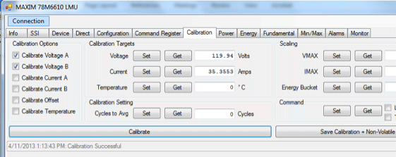
Figure 9. Voltage calibration GUI setup.
Step 3: Calibration of Current Channels
In a split-phase system (180° phase), with a balanced load, the current in the neutral is, in theory, zero (refer to the Split-Phase System Considerations section for details). To provide a non-zero signal to the Neutral sensor, a simple solution is to set the current in phase A to zero by either opening the load or by using a programmable load. In this case, the neutral current equals the current on phase B. See Figure 10.

Figure 10. Current calibration setup.
In our example (shown in Figure 11), the power meter reports a current of 0.6052ARMS, thus the corresponding value is set in the current target register. The user should then select the current channels to calibrate and issue the calibration command. The current IN = IB, therefore the current channels can be calibrated simultaneously.

Figure 11. Current calibration GUI setup.
With the inputs configured as direct slot inputs, once load A is reconnected, the current on the shunt (IA) should approach zero (assuming 180° phase and balanced source and load). See Figure 12.

Figure 12. Measurement outputs during calibration.
Step 4: Setting the Voltage and Current Channels in the Final Configuration
After calibration, the inputs must be configured to allow the proper readings of the voltage and currents in the system configuration. See Figures 13 and 14.

Figure 13. Input channels (slots) final configuration.
Once the channels are set in the final configuration, the GUI reports the correct measurements:
- IA = RMS current flowing in phase A, reconstructed based on IN (shunt/neutral current) and IB measurements.
- IB = RMS current flowing in phase B (measured with CT).
- VA = RMS voltage measured referenced to neutral.
- VB = RMS voltage measured referenced to neutral.
- VC = RMS voltage measured between VA and VB.

Figure 14. Measurements in the final configuration.
Note that the output registers are automatically scaled by a factor of ½ if the corresponding configuration registers are both non-zero, as is true in our case for IA and VC. This scaling is automatically done to prevent the output registers from overflowing.
IA is automatically scaled by a factor of 0.5 since the multiplier for S1 and S3 are both non-zero.
The resulting current is then:
IA = ((-1 × S1) + (-1 × S3))/2
Similarly for the voltage VC:
VC = ((+1 × S0) + (-1 × S2))/2
Step 5: Storing the Newly Calculated Coefficients into Flash as Defaults
The calibration coefficients, channels configuration and system defaults can be stored in the on-chip flash memory to be used as defaults. See Figure 15.
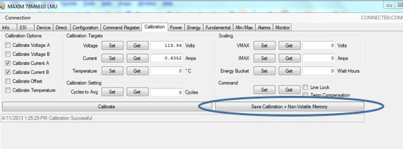
Figure 15. GUI flash save command.
Split-Phase System Considerations
Figure 16 represents a generic split-phase system. A split-phase system is commonly a 3-wire single-phase where the two hot conductors' (A, B) waveforms have a 180° phase offset.

Figure 16. Split phase system.
The voltage VA, VB, and VC relationship is the following:
- VA = Vsin(Φ)
- VB = Vsin(Φ + π)= -V(Φ)
- VC = VA - VB = 2Vsin(Φ)
For the currents:
- IN = IA + IB
With a balanced load IA = -IB therefore IN = 0
- IN = IA + IB = IA - IA = 0Ω
A split-phase system can also be derived from a 3-phase system where A and B are two of the phases and N is the neutral or star center. In this case, phases A and B have a 120° phase offset. The relationship of voltage and currents in this case are:
- VA = Vsin(Φ)
- VB = V(sin(Φ + 2/3π) = -(Vsin(Φ))/2 + √3/2 cos(Φf))
- VC = VA - VB = √3Vsin(Φ - π/6)
For balanced currents, with simple mathematical steps:
- IN = IA + IB = VA/RL + VB/RL = (V/RL)sin(Φ + π/3)