Objective
The purpose of this activity is to investigate the operation of the enhancement mode NMOS transistor as a current mirror.
Background
In terms of theory, the n-type metal-oxide-semiconductor (NMOS) current mirror operates the same as the bipolar junction transistor (BJT) current mirror that we analyzed in the August 2020 StudentZone article. Two identical transistors with the same gate-to-source voltage (VGS) will have the same drain current, ID. The second transistor, M2, in effect mirrors the current in the first, M1. Remember the drain current to gate source voltage relationship for a MOS transistor:

where K = μnCox/2 and λ can be taken as process technology constants.
Identical transistors have, by definition, the same W/L and process technology constants. In the simple current mirror, both transistors have the same VGS. Thus, both transistors will have the same ID. Since no current flows in, the gate terminal of a FET IIN = IOUT.
Materials
- ADALM2000 Active Learning Module
- Solderless breadboard
- Jumper wires
- Two 1 kΩ resistors (values matched as close as possible or measured to three digits or better)
- Two small signal NMOS transistors (ZVN2110A or CD4007 NMOS array)
- One dual op amp such as the ADTL082
- Two 4.7 μF decoupling capacitors
Directions
One good way to measure the characteristics of a current mirror is shown in Figure 1. The input and output resistors R1 and R2 are now both 1 kΩ. Be sure to accurately measure the actual values of R1 and R2 to ensure accurate measurement of the input and output current of the mirror. IIN will be equal to the W2 output voltage at W1 divided by the value of R1. IOUT will be the voltage measured by Scope Channel 2 divided by the value of R2. Diode connected M1 is connected across the gate and source terminals of M2.
In the current mirror configuration, the op amp serves as a virtual ground at the mirror input node to convert the voltage steps from W2 into current steps through the 1 kΩ resistor.


Hardware Setup
Load the stairstep.csv file for the W2 channel of the signal generator and set the amplitude to 3 V p-p with the offset to 1.5 V. The VDS of output device M2 is measured differentially by Scope Input 1+ and Scope Input 1–. The mirror output current is measured by Scope Input 2+ and Scope Input 2– across the 1 kΩ resistor, R2. The drain voltage is swept using a triangle waveform from AWG 1 (output W1) with 40 Hz frequency. If you are using the op amp setup, make sure that the device is properly connected to the power supplies Vp (5 V) and Vn (–5 V).


Procedure
Configure the oscilloscope instrument to capture several periods of the input signal and the output signal. If you are using the op amp configuration, make sure that the power supplies are turned on.
Plot the two waveforms using the oscilloscope provided by the Scopy tool or via LTspice® simulation. Examples are provided in Figure 5 and Figure 6.

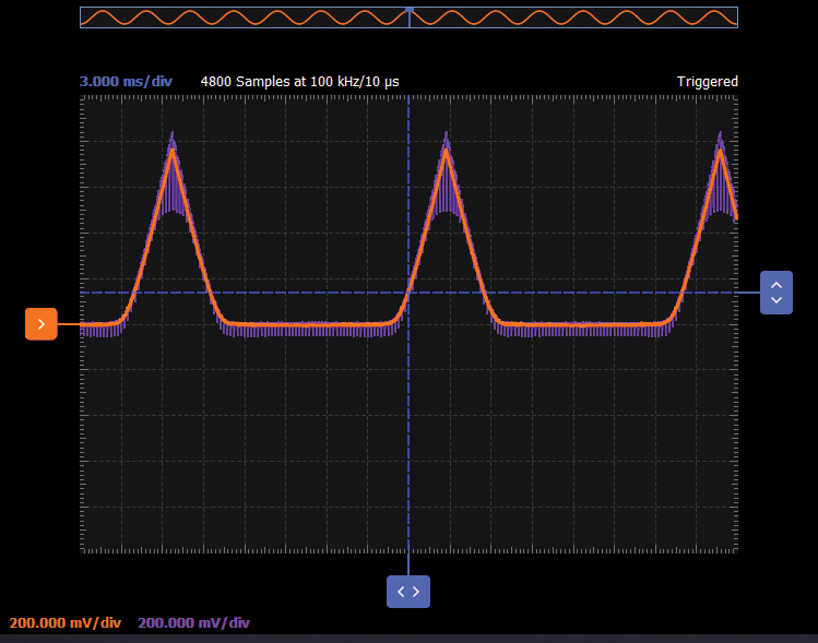
Now change the frequency of W1 at 200 Hz and plot the two waveforms. An example using an LTspice simulation of the same circuit is provided in Figure 6.


In this activity, we analyzed, both by experiment and simulation, the current mirror circuit using NMOS transistors, showcasing the usage of the ADALM2000 and the Scopy application when building real circuits.
Question
Can you name an advantage that the NMOS current mirror has over the BJT current mirror?
You can find the answer at the StudentZone blog.

