Objective:
The goal of this activity is to study the bipolar junction transistor (BJT) current source or current mirror. Important attributes for current sources include high output resistance with a wide range of voltage compliance and rejection of external variations such as power supply or temperature.
Background
A current mirror is a circuit block that functions to produce a copy of the current flowing into or out of an input terminal by replicating the current in an output terminal. The simple two-transistor implementation of the current mirror is based on the fundamental relationship that two equal size transistors at the same temperature with the same VBE have the same drain or collector current. An important feature of the current mirror is a relatively high output resistance that helps keep the output current constant regardless of load conditions. Another feature of the current mirror is a relatively low input resistance that helps to keep the input current constant regardless of drive conditions. The current being copied can be, and often is, a varying signal current. The current mirror is often used to provide bias currents and active loads in amplifier stages.
Materials:
- ADALM2000 active learning module
- Solderless breadboard
- Jumper wires
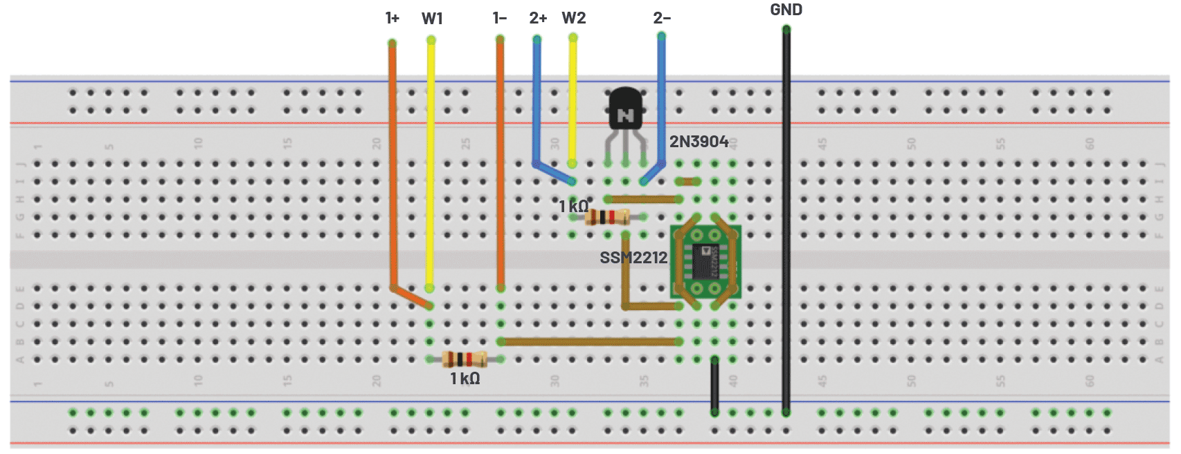
- Two 1 kΩ resistors (values matched as closely as possible, or measured to three digits or better)
- Two small signal NPN transistors (2N3904 or SSM2212)
- One dual op amp (such as ADTL082)
- Two 4.7 µF decoupling capacitors
Directions
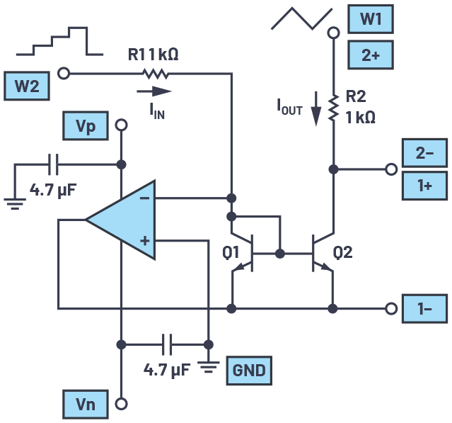
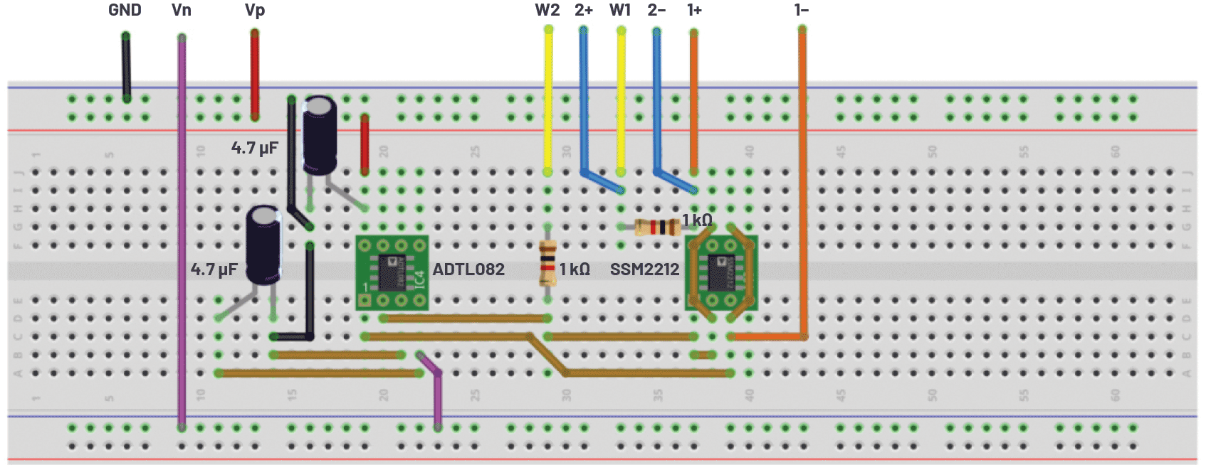
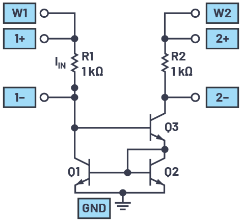
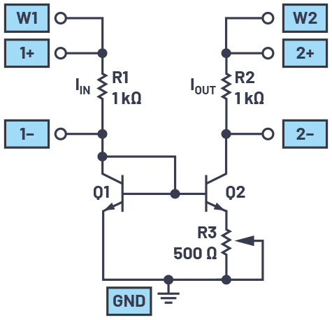
A good way to measure the characteristics of the current mirror is to reuse the same basic configuration that was used in the common-emitter BJT curve tracer experiments. The input and output resistors R1 and R2 are now both 1 kΩ. Be sure to accurately measure (with the most significant figures possible) the actual values of R1 and R2. This is to ensure accurate measurement of the input and output current of the mirror. IIN will be equal to the AWG2 output voltage at W1 divided by the value of R1. IOUT will be the voltage measured by Scope Channel 2 divided by the value of R2. Diode connected transistor Q1 is connected across the base and emitter terminals of Q2.
In the current mirror configuration, the op amp serves as a virtual ground at the mirror input (base) node to convert the voltage steps from AWG2 (W2) into current steps through the 1 kΩ resistor.

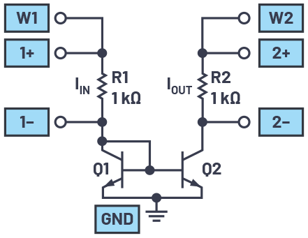
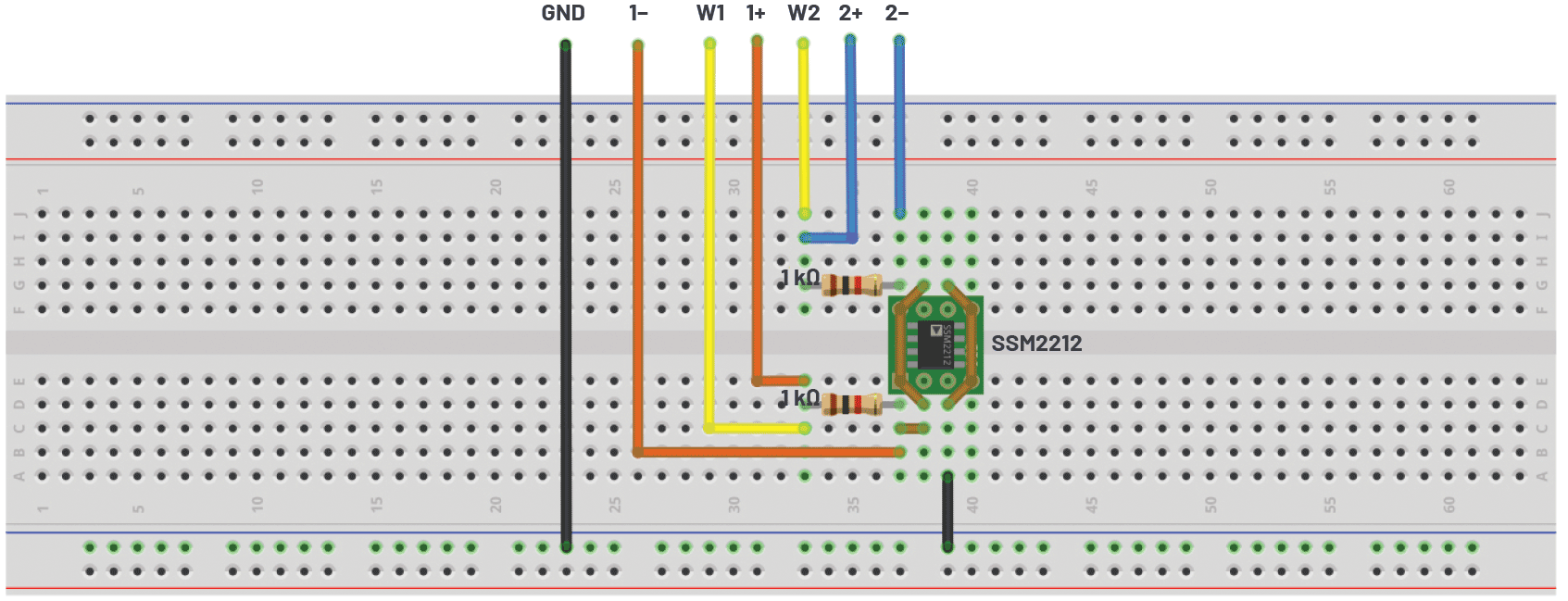
If you don’t want to use the op amp configuration, the simplified configuration shown in Figure 2 can be used as well.

Hardware Setup
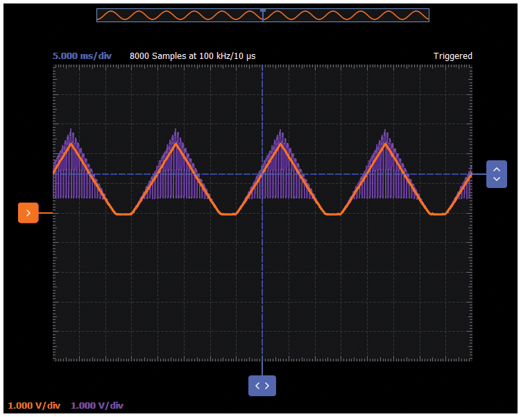
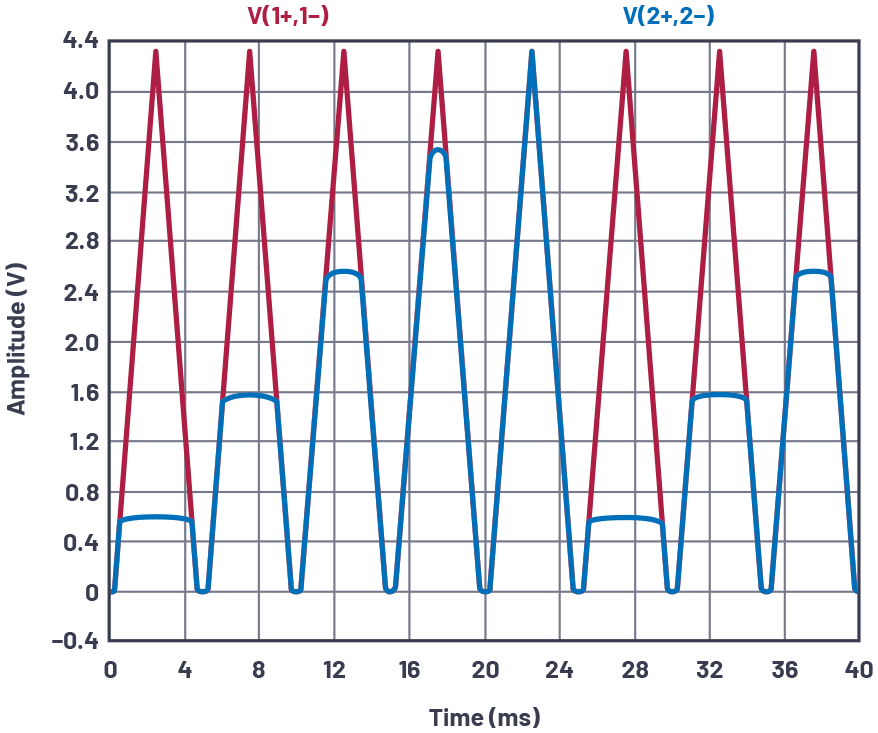
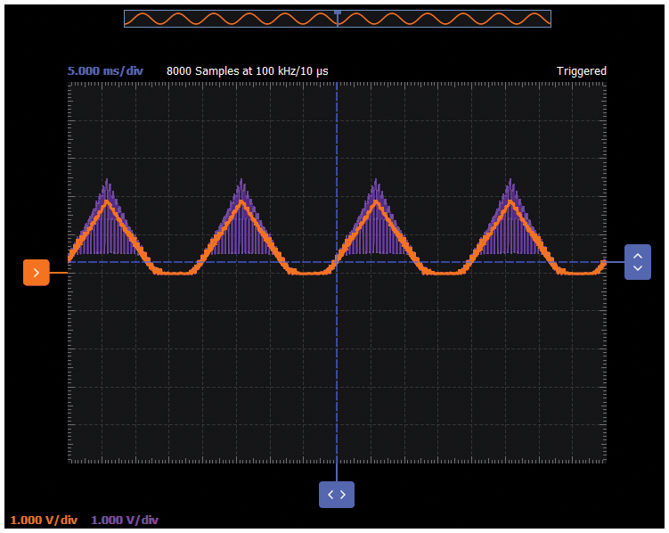
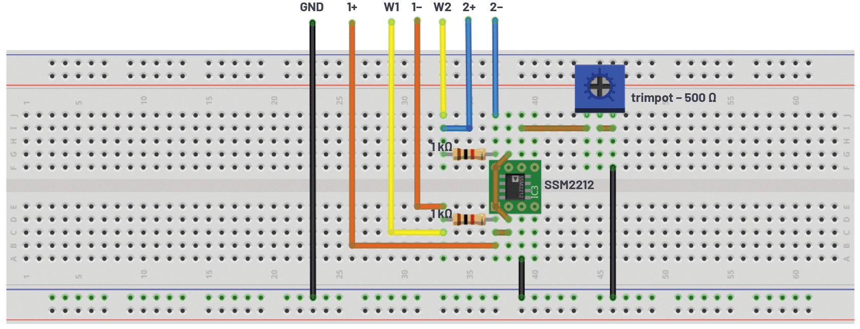
Load the stairstep.csv file for the W2 channel of the signal generator, and set the amplitude to 3 V p-p with the offset set to 1.5 V. VCE of output device Q2 is measured differentially by scope inputs 1+ and 1–. The mirror output current is measured by scope inputs 2+ and 2– across 1 kΩ resistor R2. The collector voltage is swept using a triangle waveform from AWG 1 (output W1) with 40 Hz frequency. If you are using the op amp setup, make sure that the device is properly connected to the power supplies Vp (5 V) and Vn (–5 V).


Procedure
Configure the oscilloscope instrument to capture several periods of the input signal and the output signal. If you are using the op amp configuration, make sure that the power supplies are turned on.
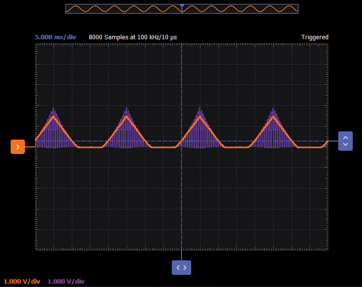
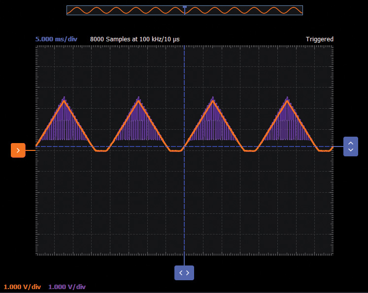
Plot the two waveforms using the oscilloscope provided by the Scopy tool or via LTspice® simulation. Examples are provided in the following figures.

Now change the frequency of W1 at 200 Hz and plot the two waveforms. An example using an LTspice simulation of the same circuit is provided in Figure 6.

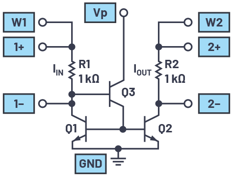
Current Mirror with Base Current Compensation
Modify the simple mirror circuit by adding the base current compensation transistor Q3 as shown in Figure 7. The simple wire connecting the collector of Q1 to its base is replaced by an emitter follower buffer. This improvement to the simple current mirror is referred to as an emitter follower augmented mirror. The current gain of the emitter follower buffer stage (Q2) greatly reduces the gain error caused by the finite base currents of Q1 and Q2.

Hardware Setup
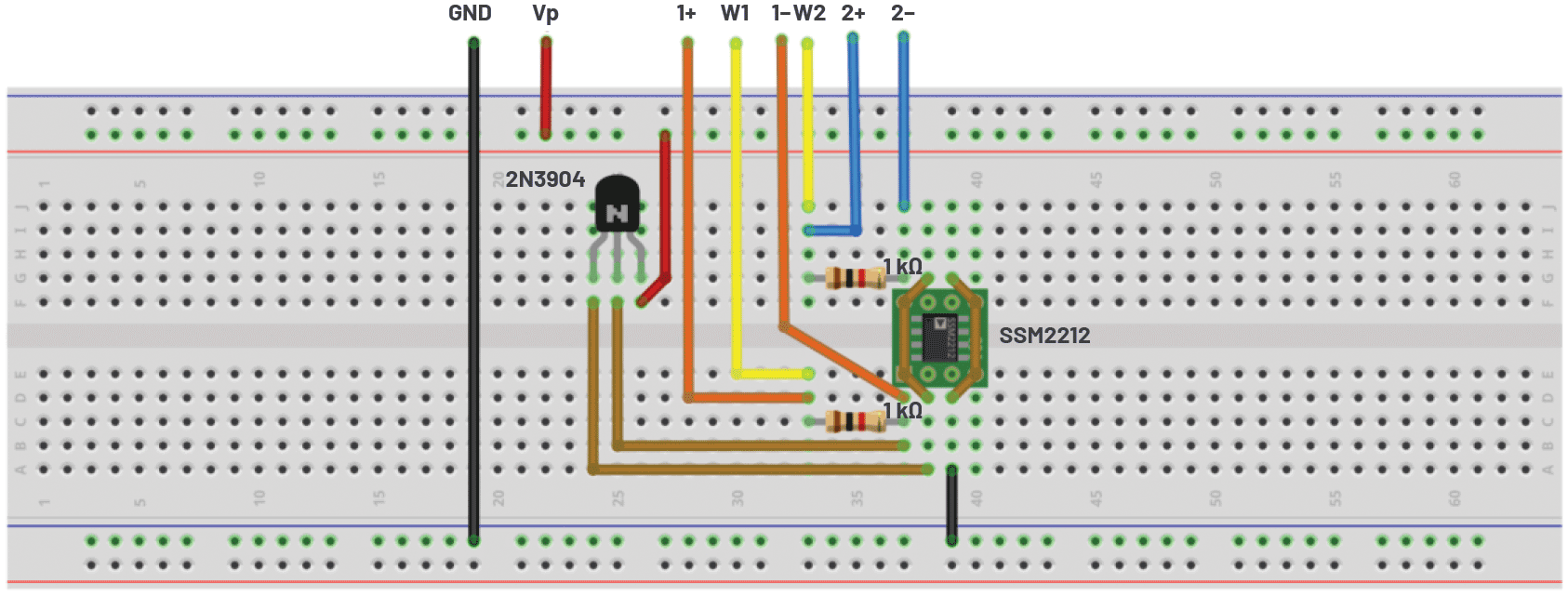
Load the stairstep.csv file for the W2 channel of the signal generator and set the amplitude to 3 V p-p with the offset set to 1.5 V. VCE of output device Q2 is measured differentially by scope inputs 1+ and 1–. The mirror output current is measured by scope inputs 2+ and 2– across 1 kΩ resistor R2. The collector voltage is swept using a triangle waveform from AWG1 (output W1) with 40 Hz frequency. Connect the positive power supply Vp (+5 V) to the collector of the Q3 transistor.

Procedure
Configure the oscilloscope instrument to capture several periods of the input signal and the output signal. Turn on the positive power supply.
Plot the two waveforms using the oscilloscope provided by the Scopy tool or via LTspice simulation. An example is provided in Figure 9.

Wilson Current Mirror
A Wilson current mirror or Wilson current source, named after George Wilson, is an improved mirror circuit configuration designed to provide a more constant current source or sink. It provides a much more accurate input to output current gain. Modify the simple mirror into a Wilson current mirror, as shown in Figure 10.

Hardware Setup
Load the stairstep.csv file for the W2 channel of the signal generator, set the amplitude to 3 V p-p with the offset set to 1.5 V. VCE of output device Q2 is measured differentially by scope inputs 1+ and 1–. The mirror output current is measured by scope inputs 2+ and 2– across 1 kΩ resistor R2. The collector voltage is swept using a triangle waveform from AWG1 (output W1) with 40 Hz frequency.

Procedure
Configure the oscilloscope instrument to capture several periods of the input signal and the output signal.
Plot the two waveforms using the oscilloscope provided by the Scopy tool or via LTspice simulation. A Scopy plot example is provided in Figure 12.

Widlar Current Mirror
Modify the simple mirror into a Widlar Mirror as shown in Figure 13. A Widlar current source is a modification of the basic two-transistor current mirror that incorporates an emitter degeneration resistor for only the output transistor, enabling the current source to generate low currents using only moderate resistor values. The Widlar circuit may be used with bipolar transistors or MOS transistors.

Hardware Setup
Load the stairstep.csv file for the W2 channel of the signal generator, set amplitude to 3 V peak-to-peak with the offset to 1.5 V. VCE of output device Q2 is measured differentially by scope inputs 1+ and 1–. The mirror output current is measured by scope inputs 2+ and 2– across 1 kΩ resistor, R2. The collector voltage is swept using a triangle waveform from AWG1 (output W1) with 40 Hz frequency.

Procedure
Configure the oscilloscope instrument to capture several periods of the input signal and the output signal.
Plot the two waveforms using the oscilloscope provided by the Scopy tool or via LTspice simulation. A Scopy plot example is provided in Figure 15.

Questions:
- Can you name one advantage and one disadvantage of the current mirror circuit with base current compensation?
- Can you name one advantage and one disadvantage of the Wilson current mirror?
You can find the answer at the StudentZone blog.

