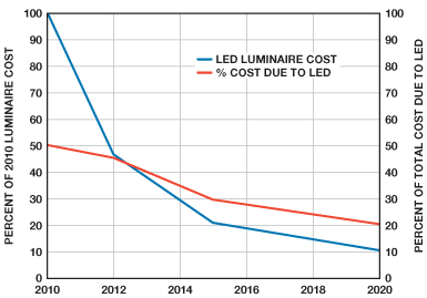
With their long lives and low energy consumption, LEDs promise to change the lighting industry, but a key limiter to rapid adoption is the cost of the LEDs themselves. The cost of LED luminaires (complete electric light units) varies, but the cost of the LED, typically around 25% to 40% of the total luminaire cost, is projected to remain significant for many years (Figure 1).
One way to reduce the total luminaire cost is to drive the LED at up to its highest possible dc current, as allowed in its datasheet. This may be considerably higher than its “binning current.” If driven properly, this can produce greater lumens/cost.
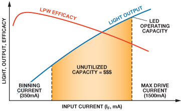
However, doing this requires higher current drivers. Many solutions are available for driving LEDs at low currents (<500 mA), but fewer options exist at higher currents (700 mA to 4 A). This may seem surprising, given that the semiconductor world is rich with dc-to-dc solutions having capacities up to 4 A, but these are designed to control voltage, not LED current. This article examines some easy tricks to transform a readily available dc-to-dc buck regulator into a smart LED driver.
A buck regulator chops an input voltage and passes it through an LC filter to provide a stable output, as illustrated in Figure 3. It employs two active elements and two passive elements. The active elements are switch “A” from the input to the inductor, and switch (or diode) “B” from ground to the inductor. The passive elements are the inductor (L) and the output capacitor (COUT). These form an LC filter, which reduces the ripple created by the active elements.
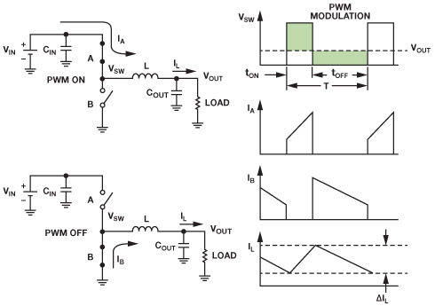
The buck is called a regulator if the switches are internal, or a controller if the switches are external. It’s synchronous if both switches are transistors (MOSFETs or BJTs) or asynchronous if the bottom switch is implemented with a diode. Each of these categories of buck circuits has its own merits and drawbacks, but synchronous buck regulators typically optimize efficiency, parts count, solution cost, and board area. Unfortunately, synchronous buck regulators for driving high-current LEDs (up to 4 A) are few and expensive. Using the ADP2384 as an example, this article shows how to modify the connections of a standard synchronous buck regulator to regulate LED current.
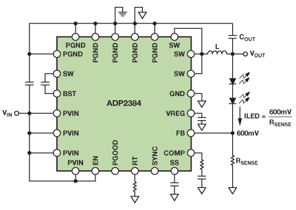
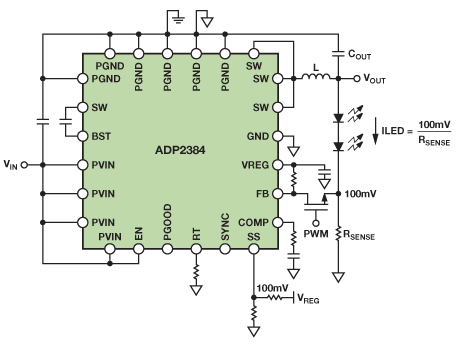
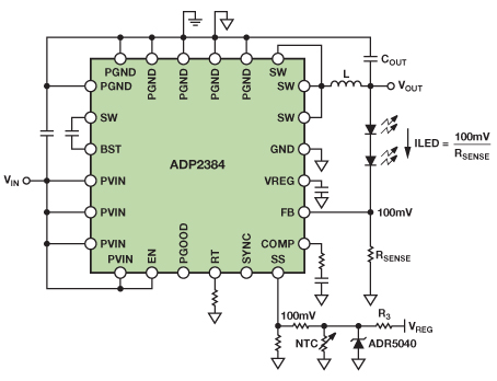
The ADP2384 high-efficiency synchronous buck regulator specifies output current up to 4 A with an input voltage up to 20 V. Figure 4 shows its normal connections for regulating output voltage.
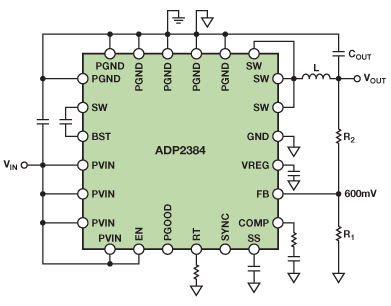
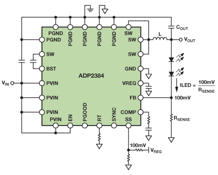
In operation, a divided down copy of the output voltage is connected to the FB pin, compared with an internal 600-mV reference, and used to generate the proper duty cycle to the switches. In the steady state, the FB pin is held at exactly 600 mV, so VOUT is regulated at 600 mV times the division ratio. If the upper resistor is replaced by LEDs (Figure 5), the output voltage must be whatever is needed (within ratings) to maintain 600 mV at FB; therefore, the current through the LEDs will be controlled at 600 mV/RSENSE.
This circuit works nicely when a precision resistor from FB to ground sets the LED current, but the resistor dissipates a lot of power: P = 600 mV × ILED. This is not a big issue for low LED currents, but at high LED currents, the low efficiency adds significantly to the heat dissipated by the luminaire (600 mV × 4 A = 2.4 W). Lowering the FB reference voltage reduces the power dissipation proportionally, but most dc-to-dc regulators do not have a means to adjust this reference. Fortunately, two tricks can reduce the reference voltage for most buck regulators: use the SS/TRK pin—or offset the RSENSE voltage.
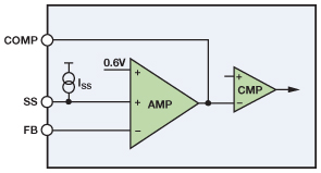
Many general-purpose buck ICs include a soft start (SS) or tracking (TRK) pin. The SS pin minimizes start-up transients by slowly increasing the switching duty cycle at startup. The TRK pin allows the buck regulator to follow an independent voltage. These functions are often combined onto a single SS/TRK pin. In most cases, the error amplifier will compare the smallest of the SS, TRK, and FB voltages with the reference, as shown in Figure 6.
For the luminaire application, set the SS/TRK pin to a fixed voltage and use it as the new FB reference. A divider from a constant voltage works nicely as a reference source. For example, many buck regulator ICs include a controlled low-voltage output—such as the VREG pin on the ADP2384. For greater accuracy, a simple 2-terminal external precision reference, such as the ADR5040, can be used. In any case, a resistive divider from that supply to the SS/TRK pin forms the new reference. Setting this voltage to between 100 mV and 200 mV generally offers the best compromise between power dissipation and LED current accuracy. Another benefit of a user-chosen reference voltage is that RSENSE can be chosen as a convenient standard value, avoiding the expense and inaccuracy of specifying or assembling an arbitrary precision resistance value to set the LED current.
Using the SS or TRK pin approach is not viable for all buck regulators, as some ICs do not have these pins. Also, with some buck ICs, the SS pin changes the peak inductor current, not the FB reference, so it is necessary to check the data sheet carefully. As an alternative, the RSENSE voltage can be offset. For example, a resistive divider between an accurate voltage source and RSENSE provides a fairly constant offset voltage from RSENSE to the FB pin (Figure 8).
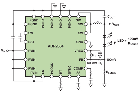
The necessary values for the resistive divider can be found using Equation 1, where VSUP is the auxiliary regulated voltage, and FBREF(NEW) is the desired voltage across RSENSE.
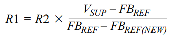
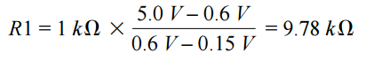
So, to get an effective feedback reference of 150 mV, with R2 = 1 kΩ and VSUP = 5 V:
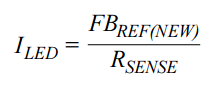
The LED current is:
This approach does not require an SS or TRK pin. The FB pin will still regulate to 600 mV (but the voltage at RSENSE regulates to FBREF(NEW)). This means that other functions of the chip (including soft start, tracking, and power good) will still function normally.
A disadvantage of this method is that the offset between RSENSE and FB is strongly influenced by the accuracy of the supply. Using a precision reference such as the ADR5040 would be ideal, but a less accurate reference tolerance of ±5% would create a ±12% variation in the LED current. A comparison is shown in Table 1:
Table 1. Comparison of SS/TRK and Offsetting RSENSE
| Option 1: Use SS/TRK to Reduce FB Reference | Option 2: Offset RSENSE Voltage |
| ±5% supply voltage variation gives ±5% error on ILED. This is not impacted by the VSENSE voltage; therefore, this method has the lowest RSENSE power dissipation. | ±5% supply voltage variation gives ±12% error on ILED. Higher VSENSE voltages improve this. |
| Very good open/short LED protection. FB_OVP does not factor into intermittent open protection. LED current is limited by the inductor and the control loop speed. | Very good open/short LED protection. Additionally, some ICs have another FB reference (FB_OVP) that immediately disables switching if FB rises 50 mV to 100 mV above normal. This guarantees the maximum LED overcurrent during intermittent faults. |
| PGOOD will always remain low. | Since FB pin still regulates to 600 mV, the PGOOD pin functions normally. |
| By keeping the SS/TRK pin lower than normal, some fault modes may not work properly. | All fault modes work normally. |
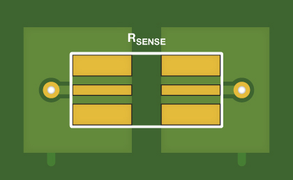
Another key for accurate current regulation is proper layout routing to the sense resistor. A 4-terminal sense resistor is ideal, but can be expensive. Good layout techniques allow high accuracy to be obtained using a traditional 2-terminal resistor, as shown in Figure 9.4
Beyond Regulating
Regulating the LED current using an off-the-shelf buck regulator is straightforward. The examples shown here employ the ADP2384. A more-extensive paper also includes examples using the ADP2441, a device with fewer pins and a 36-V input voltage range. It shows examples illustrating how to implement many of the “smart” features that are available with dedicated LED buck regulators, such as LED short/open fault protection, RSENSE open/short fault protection, PWM dimming, analog dimming, and current foldback thermal protection. We will discuss PWM and analog dimming, and current foldback here, using the ADP2384 as in the above examples.
Dimming with PWM and Analog Control
A key requirement for a “smart” LED driver is adjusting the LED brightness with dimming controls, using one of two approaches: PWM and analog. PWM dimming controls the LED current by adjusting the pulse duty cycle. If the frequency is above about 120 Hz, the human eye averages these pulses to produce a perceived average luminosity. Analog dimming scales the LED current at a constant (dc) value.
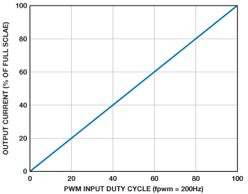
PWM dimming could be implemented by opening and closing an NMOS switch inserted in series with RSENSE. These current levels would require a power device, but adding one of these would defeat the size and cost benefits obtained by using a buck regulator containing its own power switches. Alternatively, PWM dimming can be performed by quickly turning the regulator on and off. At low PWM frequencies (<1 kHz), this can still give great accuracy (Figure 10).
Like all general-purpose buck regulators, the ADP2384 doesn’t have a pin to apply a PWM dimming input, but the FB pin can be manipulated to enable and disable switching. If FB goes high, the error amplifier goes low, and the buck switching stops. If FB is reconnected to RSENSE, then it resumes normal regulation. This can be done with either a low-current NMOS transistor or a general-purpose diode. In Figure 11, a high PWM signal connects RSENSE to FB, enabling LED regulation. A low PWM signal turns the NMOS off, with a pull-up resistor bringing FB high.
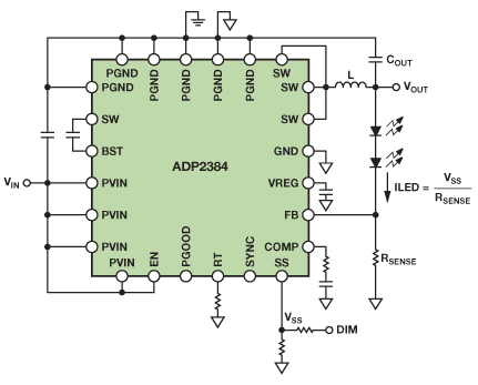
PWM dimming is very popular, but sometimes noiseless “analog” dimming is required. Analog dimming simply scales the constant LED current, whereas PWM dimming chops it. Analog dimming is required if two dimming inputs are used, since multiple PWM dimming signals can create beat frequencies that cause flicker or audible noise. However, PWM might be used for one dimming control and analog for another. With a general-purpose buck regulator, the easiest way to implement analog dimming is to manipulate the FB reference by adjusting the supply for the FB reference circuit, as described in Figure 12.
Thermal Foldback
Since the lifetime of an LED is heavily dependent on its operating junction temperature, it is sometimes necessary to monitor the LED temperature and respond if the temperature is too high. An abnormally high temperature could be caused by a poorly connected heat sink, an unusually hot ambient, or some other extreme condition. A common solution is to reduce the LED current if the temperature exceeds some threshold (Figure 13). This is called LED thermal foldback.
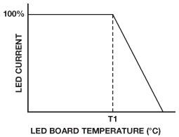
In this type of dimming, the LEDs are kept at full current until a temperature threshold (T1) is reached, above which the LED current starts to decrease with increasing temperature. This limits the junction temperature of the LEDs and preserves their lifetime. A low cost NTC (negative temperature coefficient) resistor is commonly used to measure the LED’s heat sink temperature. With a small modification to the analog dimming scheme, the NTC’s temperature can easily control the LED current. If the SS/TRK pin is used to control the FB reference, a simple method is to place the NTC in parallel with the reference voltage (Figure 14).
As the heat sink temperature rises, the NTC resistance drops. The NTC forms a resistive divider with R3. If the divider’s voltage is above the reference voltage, maximum current is delivered; if the NTC resistor voltage drops below the reference voltage, then the FB reference voltage, and hence, the LED current, starts to drop.
Conclusion
These tips should be taken as general guidelines for implementing comprehensive LED features using a standard buck regulator. However, since these features are a little outside of the intended application for the buck IC, it is always best to contact the semiconductor manufacturer for assurance that the IC can handle these modes of operation. For more information on the ADP2384 and other buck regulators, such as the ADP2441, or for demo boards of these LED driver solutions, please visit our lighting technology solutions.
I invite you to comment on Smart LED Drivers in the Analog Dialogue Community on EngineerZone.
References
1DOE SSL 2011 Manufacturing Roadmap. http://ssl.energy.gov.
2Cox, David, Don Hirsh, and Michael McClintic. “Are you using all of the lumens that you paid for?” LED Magazine, Feb. 2012.
3Marasco, Ken. “How to Apply DC-to-DC Step-Down (Buck) Regulators Successfully.” Analog Dialogue, Vol. 45, No. 2 (2011).
4O’Sullivan, Marcus. “Optimize High-Current Sensing Accuracy by Improving Pad Layout of Low-Value Shunt Resistors.” Analog Dialogue, Vol. 46, No. 2 (2012).
