ADUCRF101
RECOMMENDED FOR NEW DESIGNSPrecision Analog Microcontroller ARM Cortex M3 with RF Transceiver
- Part Models
- 3
- 1ku List Price
- Starting From $4.70
Part Details
- Analog I/O
- 6-Channel 12-bit SAR ADC
Single-ended and differential inputs
Programmable data rate up to 167 kSPS
On-chip voltage reference
Supply rante: 2.2V to 3.6V - Power Consumption
280 nA, in power-down mode, nonretained state
1.9 µA, in power-down mode, processor memory and transceiver memory retained - 210 µA/Mhz, Cortex-M3 in active mode
12.8 mA transceiver in receive mode, Cortex-M3 in power-down mode
9 mA to 32 mA transceiver in transmit mode, Cortex-M3 in power-down mode - RF Transceiver
Frequency bands, 862 MHz to 928 MHz and 431 MHz to 464 MHz
Multiple Configurations supported
Receiver sensitivity (BER), −107.5 dBm at 38.4 kbps, 2FSK
Single and ended and differential PA
Low external BOM
- Microcontroller
32-bit ARM Cortex-M3 processor
Serial Wire download and debug
External Watch crystal for wakeup timer
16 MHz internal Oscillator with 8-way Programmable Divider - Memory 128 kB Flash/EE memory, 16 kB SRAM
10,000-cycle Flash/EE endurance
10-year Flash/EE retention
In-circuit download via serial wire and UART - On-Chip Peripherals
- UART, I2C and SPI Serial I/O
28-pin GPIO port
2 general-purpose, 16-bit timers
32-bit wake-up timer
16-bit watchdog timer
8-channel pulse-width modulation (PWM) - Package
64-lead, 9 mm × 9 mm LFCSP
Temperature range: −40°C to +85°C - Tools
Low cost development system
Third-party compiler and emulator tool support
The ADuCRF101 is a fully integrated, data acquisition solution that is designed for low power, wireless applications. It features a 12-bit analog-to-digital converter (ADC), a low power ARM Cortex™-M3 processor, a 862 MHz to 928 MHz and 431 MHz to 464 MHz RF transceiver, and Flash®/EE memory. The ADuCRF101 is packaged in a 9 mm × 9 mm LFCSP.
The data acquisition section consists of a 12-bit SAR ADC. The six inputs can be configured in single-ended or differential mode. When configured in single-ended mode, they can be used for ratiometric measurements on sensors that are powered, when required, from the internal low dropout regulator (LDO). An internal battery monitor channel and an on-chip temperature sensor are also available.
This wireless data acquisition system is designed to operate in battery-powered applications where low power is critical. The device can be configured in normal operating mode or different low power modes under direct program control. In flexi mode, any peripheral can wake up the device and operate it. In hibernate mode, the internal wake-up timer remains active. In shutdown mode, only an external interrupt can wake up the device.
The ADuCRF101 integrates a low power ARM Cortex-M3 processor. It is a 32-bit RISC machine, offering up to 1.25 DMIPS peak performance. The ARM Cortex-M3 processor also has a flexible 14-channel direct memory access (DMA) controller that supports communication peripherals, serial peripheral interface (SPI), UART, and I2C. Also provided on chip are 128 kB of nonvolatile Flash/EE memory and 16 kB of SRAM.
A 16 MHz on-chip oscillator generates the system clock. This clock can be internally divided for the processor to operate at a lower frequency, thus saving power. A low power, internal 32 kHz oscillator is available and can be used to clock the four timers, as follows: two general-purpose timers, a wake-up timer, and a system watchdog timer.
A range of communication peripherals can be configured, as required, in a specific application. These peripherals include UART, I2C, SPI, GPIO ports, PWM, and RF transceivers.
The RF transceiver communicates in the 862 MHz to 928 MHz and 431 MHz to 464 MHz frequency bands using multiple configurations.
On-chip factory firmware supports in-circuit serial download via the UART, and nonintrusive emulation and program download are also supported via the serial wire interface. These features are incorporated into a low cost development system supporting this precision analog microcontroller family.
The ADuCRF101 operates from 2.2 V to 3.6 V and is specified over an industrial temperature range of −40°C to +85°C. It is available in a 64-lead LFCSP package
Applications
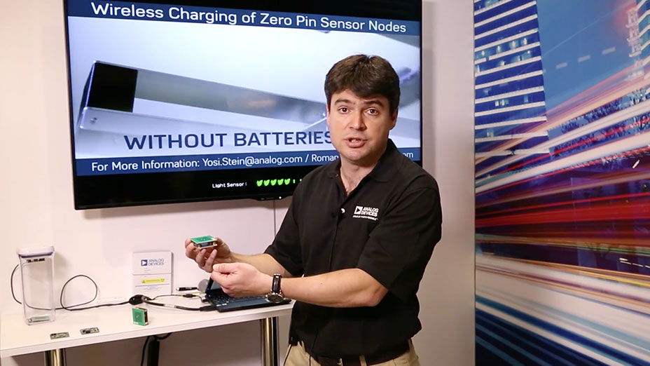
- Battery powered wireless sensor
- Medical telemetry systems
- Industrial and home automation
- Asset tracking
- Security systems (access systems)
- Health and fitness applications
Documentation
Data Sheet 1
User Guide 3
Application Note 1
Technical Articles 2
Video 8


Circuit Note 1
ADI has always placed the highest emphasis on delivering products that meet the maximum levels of quality and reliability. We achieve this by incorporating quality and reliability checks in every scope of product and process design, and in the manufacturing process as well. "Zero defects" for shipped products is always our goal. View our quality and reliability program and certifications for more information.
| Part Model | Pin/Package Drawing | Documentation | CAD Symbols, Footprints, and 3D Models |
|---|---|---|---|
| ADUCRF101BCPZ128 | 64-Lead LFCSP (9mm x 9mm w/ EP) | ||
| ADUCRF101BCPZ128R7 | 64-Lead LFCSP (9mm x 9mm w/ EP) | ||
| ADUCRF101BCPZ128RL | 64-Lead LFCSP (9mm x 9mm w/ EP) |
| Part Models | Product Lifecycle | PCN |
|---|---|---|
|
Jun 26, 2023 - 23_0025 Package Outline Drawing and Data Sheet Revision for Select LFCSP Products in Amkor |
||
| ADUCRF101BCPZ128 | PRODUCTION | |
| ADUCRF101BCPZ128R7 | PRODUCTION | |
| ADUCRF101BCPZ128RL | PRODUCTION | |
This is the most up-to-date revision of the Data Sheet.
Software Resources
Can't find the software or driver you need?
Request a Driver/SoftwareEvaluation Kits

Wireless Sensor Network (WSN) Development Kits for Your IoT Solutions
Resources


ADuCRF101 Development Systems
Resources
Software
Reference Designs

A Battery Powered Wireless Wind Speed and Wind Direction Data Acquisition System