ADL5335
RECOMMENDED FOR NEW DESIGNS700 MHz to 4200 MHz Tx DGA
- Part Models
- 2
- 1ku List Price
- Starting From $10.66
Part Details
- Differential input to single-ended output conversion
- Broad input frequency range: 700 MHz to 4200 MHz
- Maximum gain: 12.0 dB typical
- Gain range of 20 dB typical
- Gain step size: 0.5 dB typical
- Glitch free, thermometer-based digital step attenuator
- Fast attack, gain switching with programmable gain step
- Matched 50 Ω inputs and output
The ADL5335 is a digital gain amplifier (DGA) optimized for use in wireless transmitters. A differential input and single- ended output facilitates a balun free connection between the broadband integrated transceivers with differential outputs and the RF gain blocks and drivers amplifiers with single-ended inputs.
The gain is programmable via a standard Analog Devices, Inc., serial peripheral interface (SPI) port from a maximum gain of 12.0 dB down to a minimum gain of −8.0 dB with a gain step size of 0.5 dB. The ADL5335 also features a fast attack function where the gain can rapidly increase or decrease by the application of a single pulse.
The use of a thermometer-based digital step attenuator (DSA) ensures that gain changes are fundamentally glitch free. The ADL5335 is packaged in a 4 mm × 4 mm, 16-lead LFCSP. A fully populated evaluation board and system demonstration platform (SDP)-based control software are available.
Applications
- RF power control and calibration in wireless transmitters
Documentation
Data Sheet 1
User Guide 1
Product Selection Guide 1
Thought Leadership Page 1
Webcast 1
ADI has always placed the highest emphasis on delivering products that meet the maximum levels of quality and reliability. We achieve this by incorporating quality and reliability checks in every scope of product and process design, and in the manufacturing process as well. "Zero defects" for shipped products is always our goal. View our quality and reliability program and certifications for more information.
| Part Model | Pin/Package Drawing | Documentation | CAD Symbols, Footprints, and 3D Models |
|---|---|---|---|
| ADL5335ACPZN | 16-Lead LFCSP (4mm x 4mm x 0.75mm w/ EP) | ||
| ADL5335ACPZN-R7 | 16-Lead LFCSP (4mm x 4mm x 0.75mm w/ EP) |
This is the most up-to-date revision of the Data Sheet.
Software Resources
Can't find the software or driver you need?
Request a Driver/SoftwareTools & Simulations
ADIsimRF
ADIsimRF is an easy-to-use RF signal chain calculator. Cascaded gain, noise, distortion and power consumption can be calculated, plotted and exported for signal chains with up to 50 stages. ADIsimRF also includes an extensive data base of device models for ADI’s RF and mixed signal components.
Open ToolS-Parameter 1
Evaluation Kits
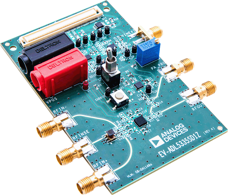


ADL5335 Evaluation Board