LTC6955
LAST TIME BUYUltralow Jitter, 7.5GHz, 11 Output Fanout Buffer Family
- Part Models
- 2
- 1ku List Price
- Starting From $10.59
Part Details
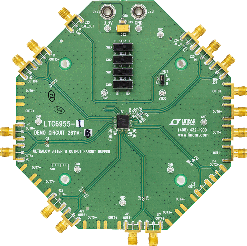
- LTC6955: 11 Output Buffer
- LTC6955-1: 10 Buffered Outputs and One ÷2 Output
- Additive Output Jitter ~45fs RMS (ADC SNR Method)
- Additive Output Jitter < 5fs RMS
- (Integration BW = 12kHz to 20MHz, f = 7.5GHz)
- Eleven Ultralow Noise CML Outputs
- Parallel Control for Multiple Output Configurations
- –40°C to 125°C Operating Junction TemperatureRange
The LTC6955 is a high performance, ultralow jitter, fanout clock buffer with eleven outputs. Its 4-pin parallel control port allows for multiple output setups, enabling any number between three and eleven outputs, as well as a complete shutdown. The parallel port also provides the ability to invert the output polarity of alternating outputs, simplifying designs with top and bottom board routing. Each of the CML outputs can run from DC to 7.5GHz. The LTC6955-1 replaces one output buffer with a divideby-2 frequency divider, allowing it to drive Analog Devices’ LTC6952 or LTC6953 to generate JESD204B subclass 1 SYSREF signals. These SYSREFs can pair with ultralow jitter device clocks from the LTC6955-1, which can run at frequencies up to 7.5GHz.
Applications
- High Performance Data Converter Clocking
- SONET, Fibre Channel, GigE Clock Distribution
- Low Skew and Jitter Clock and Data Fanout
- Wireless and Wired Communications
- Single-Ended to Differential Conversion
Documentation
Data Sheet 1
User Guide 3
Product Selection Guide 1
ADI has always placed the highest emphasis on delivering products that meet the maximum levels of quality and reliability. We achieve this by incorporating quality and reliability checks in every scope of product and process design, and in the manufacturing process as well. "Zero defects" for shipped products is always our goal. View our quality and reliability program and certifications for more information.
| Part Model | Pin/Package Drawing | Documentation | CAD Symbols, Footprints, and 3D Models |
|---|---|---|---|
| LTC6955IUKG-1#PBF | 52-Lead QFN (7mm x 8mm x 0.75mm w/ EP) | ||
| LTC6955IUKG-1#TRPBF | 52-Lead QFN (7mm x 8mm x 0.75mm w/ EP) |
| Part Models | Product Lifecycle | PCN |
|---|---|---|
|
Mar 20, 2024 - 23_0089 Obsolescence of Tower Fab3 (JAZZ-3) SBC35 Process |
||
| LTC6955IUKG-1#PBF | ||
| LTC6955IUKG-1#TRPBF | ||
This is the most up-to-date revision of the Data Sheet.
Software Resources
Can't find the software or driver you need?
Request a Driver/SoftwareHardware Ecosystem
| Parts | Product Life Cycle | Description |
|---|---|---|
| ADCLK944 | RECOMMENDED FOR NEW DESIGNS | 2.5 V/3.3 V, Four LVPECL Outputs, SiGe Clock Fanout Buffer |
| ADCLK948 | RECOMMENDED FOR NEW DESIGNS | Two Selectable Inputs, 8 LVPECL Outputs SiGe Clock Fanout Buffer |
| HMC7043 | RECOMMENDED FOR NEW DESIGNS |
High Performance, 3.2 GHz, 14-Output Fanout Buffer with JESD204B/JESD204C |