Power Module Land Grid Array (LGA) Packaging and Its Applications
Abstract
This application note discusses Analog's power module LGA packages, and provides PCB design and board assembly process guidelines.
Introduction
Analog's power module offerings come in the form of thick LGA packages on a laminate substrate.
The constituent elements of the package are:
- Controller die and FET die
- Ceramic chip capacitors
- Thick-film chip resistors
- Inductor
All components are encapsulated by a mold compound to form a flat surface at the package top-side. A representative image of the package cross-section is shown in Figure 1.

Figure 1. Power module LGA package construction (not to scale).
Two-layer laminate substrates are used for these LGA modules. CCL-HL832NX (from MGC) is the core material of choice and the solder mask is PSR4000 (from Taiyo). The substrate cross-section is shown in Figure 2 below.

Figure 2. Substrate cross-section.
A representative package outline drawing (POD) of one of Analog's power modules is provided in Figure 3.
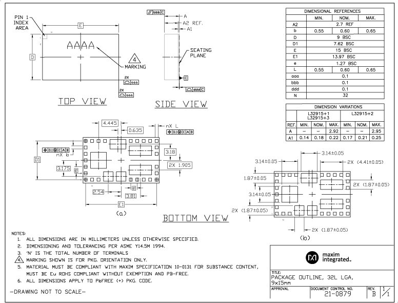
Figure 3. Package outline drawing of the 9mm x 15mm LGA package.
PCB Design
Analog LGA packages use solder-mask-defined (SMD) pins. Pins at the periphery are the signal pins, while the larger internal pins are for thermal lands. Two types of land patterns are used for surface-mount devices:
- Solder Mask-Defined (SMD) pads have solder mask openings that are smaller than metal pads.
- Non-Solder Mask-Defined (NSMD) pads have solder mask opening that are larger than the metal pads.
Analog recommends the use of NSMD pads because of the following advantages: (i) The copper etching process has better control compared to solder masking and, (ii) NSMD provides a large metal area for the solder to anchor to (pad area + vertical edges of pad).
IPC-7351 guidelines can be used to design PCB pad patterns based on the package outline drawings for the respective ages. The IPC land pattern calculator can be downloaded from IPC website (www.ipc.org)
For NSMD
PCB pad dimensions are recommended to be 0.1mm larger than those of the LGA pins (0.05mm extension on either side)—for signal pins as well as thermal pads. Use PCB pad dimension +0.2mm as minimum solder mask opening for each pad.
For SMD
Use LGA pin dimension +0.1mm as recommended solder mask opening for each PCB pad. PCB pad dimensions should be minimum 0.25mm larger than those of the LGA pins (0.125mm extension on either side)—for signal pins as well as thermal pad.

Figure 4. Illustration of NSMD and SMD land pad patterns.
PCB Surface Finish
The selection of an appropriate PCB pad surface finish is critical to ensuring optimum manufacturing of the final board assembly. Popular surface finishes for PCB pads are listed below:
- OSP (Organic Solderability Preservative)—Recommended
- ENIG (Electroless Nickel, Immersion Gold)—Recommended
- Electroplated Nickel, Gold
- Immersion Ag
- Immersion Sn
Stencil Design
The stencil thickness and pattern geometry determine the precise volume of solder paste deposited onto the device land pattern. Stencil alignment accuracy, as well as consistent solder volume transfer, is critical for uniform solder reflow. Stainless steel stencils are preferred. Stencils should be laser-cut and then electro-polished for better release than the regular laser-cut stencil.
The recommended stencil thickness is 5mils (0.125mm).
The stencil opening should be designed to be 1 mil (25µm) per side smaller than the PCB pad size. The tolerances must be tightly controlled as they can effectively reduce aperture size. Walls of the apertures should be: (i) smooth, (ii) with rounded corners, and (iii) trapezoidal cross-section (bottom opening larger than top) to enhance the release of solder paste from the aperture. Stencil aperture must meet the industry-standard area ratio of (Area of aperture opening/Aperture wall area) > 0.66.
Smaller multiple openings should be used instead of a large, single opening (see Figure 5 below). 60% to 80% solder paste coverage is recommended. Rounded corners should be used to minimize solder paste clogging. Final solder joint thickness for LGA terminal pads should be 50µm–75µm.

Figure 5. Stencil design recommendation.
Solder Paste
A low-residue, no-clean solder paste is recommended for mounting LGA packages. Type III or IV solder pastes are best suited for the typical pitch used in Analog's modules. Nitrogen purge is recommended during solder reflow. Follow paste supplier's recommended stencil clean frequency for respective solder pastes.
- Recommended solder paste compositions are shown below:
- Lead-free(Recommended): SAC (Sn-Ag-Cu) alloys (SAC305)
- Lead-based: Sn/Pb alloys (Sn63Pb37)
Screen Printing
A metal squeeze should be used with 45° to 60° print angle. For printing, 20mm/sec should be used as a starting speed; speed can be further increased as comfortable. Pressure of ~10N/mm should be applied with the squeeze while printing. The snap of distance should be 0mm. Also, it is recommended to do a post-printing solder inspection to check for print quality.
Placement
A standard pick and place machine with 0.05mm accuracy can be used for placing the LGA modules on the printed solder. Low mounting speed is recommended to prevent the paste from squeezing out. The package should be pushed 1~2 mils inside the paste to achieve good contact of LGA pad and solder.
LGAs have a capability to self-align so long as 75% of the LGA pin overlaps with the PCB pad.
Reflow
It is recommended to use a forced convection oven with nitrogen, having a temperature uniformity within ±5°C. Reflow profile guidelines from the solder paste’s data sheet should be followed. The guidelines are based on the temperature at the actual joint location; the actual temperature of the solder joint often differs from the temperature settings in the reflow system, depending on board density, board thickness, and other parts mounted on the board. It is recommended that the profiles be checked using thermocouples at the actual solder joint locations prior to being used for the actual board interconnection reflow. Figure 6 shows the recommended reflow profile for Pb-free solders per JEDEC JSTD-020.
Double-sided reflow should not be performed for these LGA modules.

Figure 6. Recommended reflow profile for Pb-free solders per JEDEC JSTD-020.
Cleaning
If low-residue, no-clean solder paste is used, cleaning is generally not required. It is recommended to follow supplier’s guidelines for cleaning. If cleaning is done, boards need to be dried later.
Rework
Component Removal
An appropriate rework station should be used for any rework on the parts. It is strongly recommended to bake the PCB assembly at 125°C for 24 hours to eliminate residual moisture before component removal. The bottom of the PCB should be heated using convective heaters, while hot air or gas is used on the top side of the component (this is to prevent warpage). A special nozzle should be used to direct the air to the component only in order to reduce heating of adjacent components. Thermocouples should be used on top and bottom side to monitor actual temperature at the part. Max part temperature should be above the liquids temperature of 217°C, but should not exceed 245°C. Once the joints have reflowed, the vacuum lift-off should be automatically engaged during the transition from reflow to cool down. The vacuum pressure should be kept below 15 inch of Hg, to ensure the component is not lifted out if all joints have not been reflowed (to prevent pad lift-off).
Site Redress
Following component removal, the PCB site should be properly cleaned, while taking care that the pads are not damaged. The PCB pads should then be cleaned with a solvent; the solvent is usually specific to the type of paste used in the original assembly and paste manufacturer’s recommendations should be followed.
Solder Paste Printing
A miniature stencil is recommended to be used to print solder paste on the PCB surface at the component site. Alternately solder paste can be printed onto the package bottom side. Follow stencil thickness, stencil design, solder recommendations and screen-printing guidelines as provided for original PCB assembly Inspect the site before replacing the new part.
Component Placement
A new replacement part should be used; it is not recommended to use the removed part. Split-beam optical system should be used to align the component on the PCB (as the leads are at the bottom of the package); this will provide an image of leads overlaid on the mating footprint and aid in proper alignment. Placement machine having 0.05mm placement accuracy should be used. Follow other placement guidelines provide in the PCB assembly art of the document.
Reflow
Same reflow profile as provided for initial component attach reflow is recommended to be used. X-ray can be used to inspect if all the joints are formed successfully.
Moisture Sensitivity
All Analog LGA modules meet MSL3 standard as per JEDEC specification JSTD020D.1.
Units Shipping
Parts will be shipped in tray or tape-and-reel form. All parts will be baked and dry-packed with desiccants and a humidity indicator card. If the humidity indicator card has turned pink, or if the parts have been exposed to longer than their floor life, packages should be subjected to bake at 125°C for 48 hours. Refer to JEDEC specification J-STD-033C for correct use of moisture/reflow sensitive surface-mount devices.