AN-2003: On-Chip Oversampling for the Analog Devices, Inc., AD7380 Family of SAR ADCs
INTRODUCTION
This application note discusses on-chip oversampling in successive approximation register (SAR), analog-to-digital converters (ADCs). Two common oversampling techniques are normal average and rolling average. These techniques are performed within the AD7380/AD7381 and its family of high throughput rate SAR ADCs so that averaged conversion data is directly available, and so that there is less of a burden on the digital controller, which is an advantage in data acquisition systems.
In a precision data acquisition system, the higher the signal-to-noise ratio (SNR) and the effective number of bits (ENOB), the better the system is at measuring the signal power in the presence of broadband noise.
Noise can degrade system performance. Some ways to reduce noise are to replace the system with a higher resolution ADC, such as an Σ-Δ ADC or SAR ADC, or to oversample and use digital filtering techniques.
The oversampling technique has a history within Σ-Δ ADCs architecture design. An Σ-Δ ADC is constructed from a Σ modulator and a subsequent digital signal processing block, or digital filter. The Σ modulator can be as small as a single bit quantizer to collect thousands of samples and then decimate those samples to achieve a high resolution conversion result. The more samples averaged, the more resolution achievable, resulting in the conversion being closer to the sampled value. Some common Σ-Δ applications are temperature monitoring and weigh scale measurement systems.
Σ-Δ ADC architectures rely on sampling smaller charge at much higher rates than the bandwidth of interest. Taking more samples but with smaller bites. The oversampling range of a typical Σ-Δ ADC falls between 32× up to 1000× the signal of interest. The outcome of oversampling combined with noise shaping (modulation scheme) moves in-band noise out of the bandwidths of interest. The noise moved to higher bandwidths then gets filtered out digitally. The outcome is lower noise and higher resolution in the bandwidth of interest. Each conversion result from the Σ-Δ ADC comes about because of smaller but more frequent sampling events.
SAR ADCs use successive approximation to determine the result. SAR ADCs use a step by step approach to establish what each bit of the digital representation is of a single sampling instant. The SAR employs a charge redistribution capacitor and a digital-to-analog converter (DAC) array. The sampled data is compared to each of the binary weighted capacitive arrays. The total number of binary weighted capacitors determines the number of bits or resolution of the SAR ADC. The conversion process is controlled by a high speed internal clock and the capacitive DAC array, which is able to rapidly convert changing signals. SAR ADCs are used in data acquisition systems that require wide bandwidths.
A SAR ADC typically converts a single instance in time providing a digital answer that relates to a specific time instant. With the advent of faster SAR converters, there is an increased usage of oversampling to improve resolutions for the key bandwidths of interest. Often today where SAR ADCs use the oversampling technique, the technique is performed via post processing on microcontrollers or the field programmable gate arrays (FPGAs). Analog Devices, Inc., offers an oversampling feature built in to its series of SAR ADCs. This oversampling feature improves noise performance, simplifies interface requirements, and allows users to employ out of the box without the need for the design and resource intensive averaging of FPGAs or microcontrollers. The oversampling features also maximizes data processing performance at a manageable data rate.
| Input Type | 16-Bit | 14-Bit | 12-Bit |
| Differential Single-Ended |
AD7380 AD7386 |
AD7381 AD7387 |
AD7388 |
OVERSAMPLING
During analog-to-digital conversion, an analog signal is digitized by an ADC. Oversampling is a technique applied to increase the effective, digitized signal resolution by sampling the analog signal and by converting this signal digitally at a much higher rate than required when compared to nonoversampling solutions. Oversampling allows users to average out the noise of the converter over a wider bandwidth. When averaged and/or filtered to a specific bandwidth, noise improves at a rate of √2, or 3 dB, for every 2× oversampling, providing that noise is uncorrelated, broadband (white) noise and zero (0) mean. Other spectral content, such as correlated noise or harmonics, is not reduced by averaging. Figure 1 shows the noise level of an ADC (dark gray) that comes from combined sources of quantization noise, thermal noise, and external noise, such as drivers, a clock, and a voltage reference, spread across the Nyquist bandwidth.


According to the Nyquist theory (fSAMPLING ≥ (2 × fIN)), the input signal must be sampled at a rate of at least twice the maximum frequency of interest for a signal to accurately reconstruct, and the same criteria is present for oversampling to occur. Oversampling reduces the noise of the signal, which leads to increases in the system SNR, and therefore, resolution improvement (assuming no significant distortion components).
Oversampling is a digital signal processing technique where several samples are collected and then averaged. Data sample averaging acts like a low-pass filter.
The Analog Devices AD7380 family is a simultaneous sampling SAR ADC family that is capable of on-chip oversampling. This SAR ADC series can perform two oversampling techniques: normal average and rolling average.
NORMAL AVERAGE OVERSAMPLING
In normal average oversampling, the average algorithm is implemented as a simple average by which M samples are added together, and then the resulting sum is divided by the same factor of M. In this method, a new set of M samples are collected for each averaged result.
Table 2 shows a general representation of how the algorithm works. In this example, the data has 12 samples. When M = 2, the number of samples averaged is two, resulting in a new output every two samples, thus at half the effective sample rate. The results are the average of Sample 1 and Sample 2, Sample 3 and Sample 4, and so on.
| Sample Number | Sample Result | Averaged Result | |
| M = 2 | M = 4 | ||
| 1 | 0.200 | 0.2500 | 0.2400 |
| 2 | 0.300 | ||
| 3 | 0.230 | 0.2350 | |
| 4 | 0.240 | ||
| 5 | 0.260 | 0.2300 | 0.2500 |
| 6 | 0.200 | ||
| 7 | 0.240 | 0.2700 | |
| 8 | 0.300 | ||
| 9 | 0.270 | 0.2600 | 0.2450 |
| 10 | 0.240 | ||
| 11 | 0.250 | 0.2300 | |
| 12 | 0.210 | ||
Similarly, applying an averaging factor of M = 4, the first set of four samples is averaged, and then another set of four samples (Sample 5 to Sample 8) is averaged. A simplified normal average equation follows:

where:
x is the average of M samples.
M is the number of samples to average.
Si is the nth sampled value.
In the AD7380 SAR ADC family, normal average oversampling implements within the chip and can collect a maximum of 32 averaging samples. Whenever this technique is enabled, the AD7380 automatically collects M number of conversion samples and then clocks out the averaged conversion result. The availability of the conversion result is dependent on the M number of samples collected, which is set by the over-sampling ratio on the OSR bits in the CONFIGURATION1 register of the AD7380 family. The result is read when the M sample conversion completes.
Figure 2 shows how the AD7380 performs the algorithm. In this example, it is assumed that M = 8 or the oversampling ratio (OSR) is 8, resulting in collection and averaging of eight samples. When the conversion initiates internally, the AD7380 erforms a series of convert and acquire processes until the requested number of samples (M) completes. Then, the averaging process executes on the captured data. As a result, some processing latency is introduced, as shown in Figure 2, and at T1, the average result is available and clocks out on the SDOx pins. At this instant, a new average operation initiates, resulting in a new conversion burst to acquire the next M samples. Figure 2 shows that applying this technique results in a reduction in the effective ODR of the sampling system. The ODR decrease is inversely proportional to the samples count (M) or increased OSR. The normal average oversampling method is recommended for applications where optimal performance is required but a slower ODR is acceptable.


ROLLING AVERAGE OVERSAMPLING
The rolling average oversampling technique uses a buffer to store samples for the averaging process. The rolling average algorithm selects the latest M samples stored in the buffer and divides the resulting sum by M. In digital designs, buffers need additional space to create additional storage. In the rolling average oversampling technique, a small ADC has a limited buffer storage capacity and employs a first in, first out (FIFO) algorithm. When the buffers are full and a new sample is available, the earliest data in the buffer is discarded, as shown in Figure 3. Using the previous example sampled data, the first eight sample results fill the FIFO buffer (S1 to S8). As new sample data (S9) is available, S1 drops off from the buffer and S9 inserts into the buffer. The same process follows through as new samples are stored in the buffer.
As previously described, the rolling average oversampling technique adds the latest M samples and computes the resulting average by dividing by M. In the example presented in Figure 3, where M = 4, the algorithm adds the four samples available in the FIFO buffer, B1 to B4, which are the latest four samples and then divides by 4. During the next average, the same FIFO buffer location is averaged, but the content in these buffers change. In a scenario where M = 8, all samples in the FIFO buffer are included in the sum operation and subsequent division by 8.


To enable rolling average oversampling in the AD7380 family, set the OS_MODE bit to Logic 1, and a valid nonzero value must be in the OSR bits in the CONFIGURATION1 register to store up to 8 samples in the FIFO buffer. The FIFO buffer updates as soon as the conversion takes place. When rolling average oversampling enables, its algorithm collects the latest M number of samples from the FIFO buffer and divides by M, where M is the OSR. The averaged result then clocks out on the SDOx pins of the AD7380.
Figure 4 shows that as soon as the samples in the buffer are available, M = 8 in this example, the oversampling result is available on the subsequent conversion cycle. Therefore, faster output data rates (ODRs), even when M (the number of samples) increases. The rolling average oversampling technique is useful in applications where high ODR and high performance are required. The achievable performance increase for this technique is limited by the available buffer storage. A simplified rolling average equation follows:

where:
x is the average of M samples.
M is the number of samples to averaged.
Bi is the sample at the specific buffer location.


OVERSAMPLING BENEFITS
NOISE IMPROVEMENT
ADCs can achieve higher dynamic range with oversampling. Oversampling works by assuming noise sources are uncorrelated and have a zero mean because samples consider white noise uniformly distributed noise across the spectrum, or Gaussian noise distribution centered around adjacent codes as signals that can be reduced by averaging.
Figure 5 is an example fast Fourier transform (FFT) plot generated using the AD7380 without oversampling and with rolling average oversampling applied and an OSR = 8.


Observe the significant improvement in the noise floor, corresponding to an increase in SNR (see Figure 6). In this example, the SNR improves to 96 dB and 95 dB with normal average oversampling and rolling average oversampling enabled, respectively.


To estimate the SNR improvement from applying the oversampling technique, use the following equation:

where:
N is the ADC resolution.
fs is the sampling frequency.
BW is the bandwidth of interest.
10log(fs/(2 × BW)) is the process gain.
fs/(2 × BW) is the sampling ratio or Nyquist ratio.
Note that the process gain is included to account for the additional oversampling process that is sampling beyond 2 × BW. In the following equation, increasing the sampling frequency by a factor k, where k is the number of samples averaged or the oversampling ratio, results in an increased SNR.

Ideally, doubling the value of k results in a 3 dB increase in SNR.
Typical normal and rolling average oversampling effects on SNR at different oversampling ratios are detailed in Table 3 and Table 4. As the oversampling ratio increases, the SNR also increases.
| Oversampling Ratio | SNR (dB) | Output Data Rate (kSPS) | |
| Reference Voltage (VREF) = 2.5 V | VREF = 3.3 V | ||
| Disabled 2× 4× 8× 16× 32× |
90.8 92.6 94.3 95.8 96.3 96.5 |
92.5 94 95.4 96.3 96.8 97 |
4000 1500 750 375 187.5 93.75 |
| Oversampling Ratio | SNR (dB) | Output Data Rate (kSPS) |
| Disabled 2× 4× 8× |
90.3 91.7 93.37 94.66 |
4000 4000 4000 4000 |
Both averaging techniques are available in the AD7380 family of generics. Each of the techniques are recommended for a range of applications. However, each of the techniques has its own attributes that must be consider for specific applications. The normal averaging oversampling technique provides the following:
- Optimal performance because this technique samples additional data for averaging.
- Slower ODR because the number of samples or OSR increases, enabling applications to use lower SCLK frequencies, which lowers the overall cost.
- Signal bandwidths significantly less than conversion rates (see Figure 7). Note that bandwidth limitations are attributed as an effective low-pass filter.


The rolling average oversampling technique provides the following:
- A sampling rate that can vary and be controlled by the application via the CS pin.
- A fast sampling rate with a maximum of 4 MSPS.
- A limit to the number of samples averaged of eight due to buffer constraints.
- A wider signal bandwidth (see Figure 7).
INCREASED RESOLUTION (N)
As previously discussed, both oversampling techniques showed significant improvement in performance. Using the following formula, SNR is limited to the N resolution of the ADC.
Use the following equation to calculate for N:

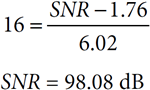
Calculating the SNR given an ideal 16-bit ADC yields a maximum SNR of 98 dB.
The maximum SNR improvement is limited by the number of bits of the ADC, which is shown in Figure 6, where there is little to no increase in SNR performance with oversampling ratios greater than 8. To get the benefit of oversampling, N resolution must be increased, which is the significance of the resolution boost feature of the AD7380.
BOOST RESOLUTION
Even with limitations, the AD7380 family can extend the achievable SNR by effectively boosting the resolution through oversampling. To enable on-chip boost resolutions, write to the RES bit (Bit 2) of the CONFIGRATION1 register.
To understand how oversampling can increase SNR, use the previous equation to compute the SNR of a 17-bit ADC. The result is a SNR of 104.1 dB.
Plugging this value into the SNR equation gives the oversampling factor, k, required to increase the resolution by 1 bit.

To increase the resolution by 1 bit, the ADC oversampling ratio must be a minimum of 4. The oversampling factor required to increase the resolution is summarized in the following equation:

Where x is the additional resolution.
Table 5 summarizes the resolution increase for different oversampling ratios.
| Oversampling Ratio | Number of Bits Increased |
| 2× 4× 8× 16× 32× |
0.5 1 1.5 2 2.5 |
Figure 8 shows the SNR performance of the AD7380 when the resolution boost is enabled. An SNR performance of more than 100 dB is achieved. The additional 2-bit resolution boost improves the quantization noise and results in an SNR increase. The resolution boost is a way of increasing the dynamic range of the system without resorting to the higher cost of an additional 2 bits of resolution. The drawback of this feature is that it requires an extra 2 clock cycles in the serial port interface (SPI) SCLK to clock out the averaged conversion result.


APPLICATION EXAMPLE
Optical encoders are used in motor control applications to capture accurate position measurement. For example, sine and cosine outputs from an encoder are interpolated and must be captured simultaneously. A simultaneous sampling SAR ADC is recommended for this type of application, for example, the high throughout rate, AD7380. The angular position, θ (theta), is obtained by the arctangent of the captured sine and cosine signals. When these signals are ideal, the results are accurate. In real-world applications, these signals can be affected by noise that results in reading errors. These deviations cause errors in the angular position of the encoder.
A high encoder accuracy demand example is when a motor runs at slower speeds, this is, when the motor starts to slow down and then reaches the target position. Use of the on-chip oversampling technique of the AD7380 enables digital filtering of the sine and cosine signals, which allows a high dynamic range. The enhanced sine and cosine conversion results in higher angular position accuracy, which is a requirement in applications, such as pick and place machines for mounting tiny component into a printed circuit board (PCB) or robotic arms in the industrial machinery for transporting and moving loads to a specific location.
CONCLUSION
Oversampling is a data processing technique that provides precision conversion results on ADCs. SAR ADCs have historically employed this technique in post processing through micro-controllers, DSPs, or FPGAs. The Analog Devices family of a high speed SAR ADCs, such as the AD7380, have integrated this functionality into two oversampling techniques on-chip, normal and rolling average. Quick access to the averaged conversion results are directly available on the SDOx pins, resulting in obvious effects that immediately manifest in ADC parameters, such as SNR and a full dynamic range.
The normal average oversampling technique is suited for applications where higher performance is a requirement and lower clock speeds and output data rates are acceptable. The rolling average oversampling technique is appropriate for applications where speed is a requirement together with performance.
The oversampling performance is further improved with increased resolution. Note that, in conjunction with the two oversampling techniques discussed, an additional 2-bit resolution can be added directly with the resolution boost feature found in the AD7380 family. The AD7380 generics are high speed SAR ADCs that relieve the burden of the SPI on the microcontroller for extra data processing, and the AD7380 family of devices are highly reliable for improved ADC conversion accuracy.
Author
