Let’s assume that you’ve read the previous November and December StudentZone columns on breadboarding and prototyping and have had some success in actually building a working circuit for a project or just for a hobby. You probably used a solderless breadboard, and the circuit may look something like the one shown in Figure 1.
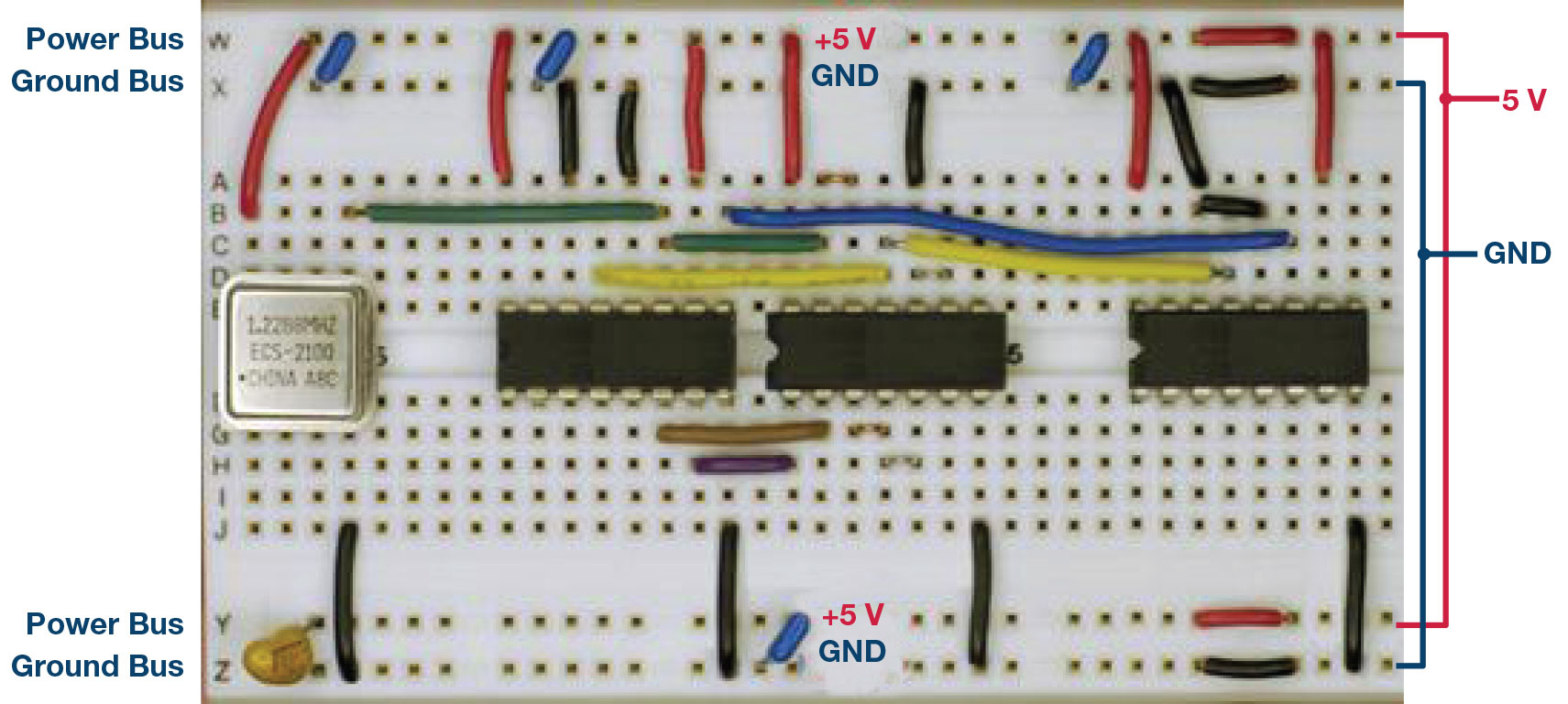
You were clever and took advantage of the buses at the top and bottom of the board and used them for the voltage and ground connections. In the Figure 1 circuit, there are two +5 V buses and two GND buses located on the top and bottom of the board (connected together with an external wire). This dual bus arrangement allows flexibility in making the power and ground connections from either half of the board. Good job!
Maybe during your time as an EE student you built several of these types of circuits and decide to take one of them to a job interview your senior year to show prospective employers your capabilities. After all, you have heard that they like to see evidence of practical experience. You bring the schematic, circuit description, and test data to the interview. The interview is going well, and you show your breadboard—but the interviewer then asks you to describe the limitations of your circuit. So you launch into the theory of the circuit and its capabilities, but the interviewer stops you and asks you to explain how you dealt with the important layout issues of grounding and decoupling. You explain how you used power and ground buses, but the interviewer asks about how you handled parasitic impedances and ground currents, and starts talking about ground and power planes, multilayer printed circuit boards, and high and low frequency decoupling; and your interview suddenly takes a turn for the worse.
Unfortunately there are no university classes offered specifically in PCB Grounding and Decoupling 101 (if you know of any, please let us know!), and any knowledge you pick up in this area will probably come from lab experience or working with instructors who are engaged in hardware development. Due to time constraints, most EE curriculums just don’t cover these important practical issues. While most EE graduates learn these skills on the job, you will really have an advantage if you are at least aware of the critical issues involved in taking a circuit design from schematic to layout and to final production on a PCB.
So we are going to cover the fundamentals in this column on grounding and the next one on decoupling to give you a head start. Please understand that these discussions only cover the basics, and there is much more material available in the various references given at the end of the column.
Perfect vs. Imperfect Grounds
Figure 2 shows signal source and a load separated by some distance where the grounds G1 and G2 are connected by a return path. Ideally the ground impedance between G1 and G2 is zero, and therefore the ground return current does not develop a differential voltage between G1 and G2.
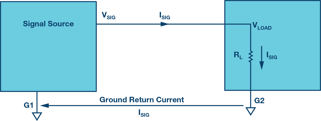
Unfortunately, it is impossible to maintain zero impedance in the current return path, and the ground return impedance allows the ground current to develop an error voltage ΔV between G1 and G2. There is not only resistance but also inductance in the connection between G1 and G2. For the purposes of this discussion we are going to neglect the effects of stray capacitance. However, in the next column you will see how capacitance between power and ground planes can actually assist in high frequency decoupling.
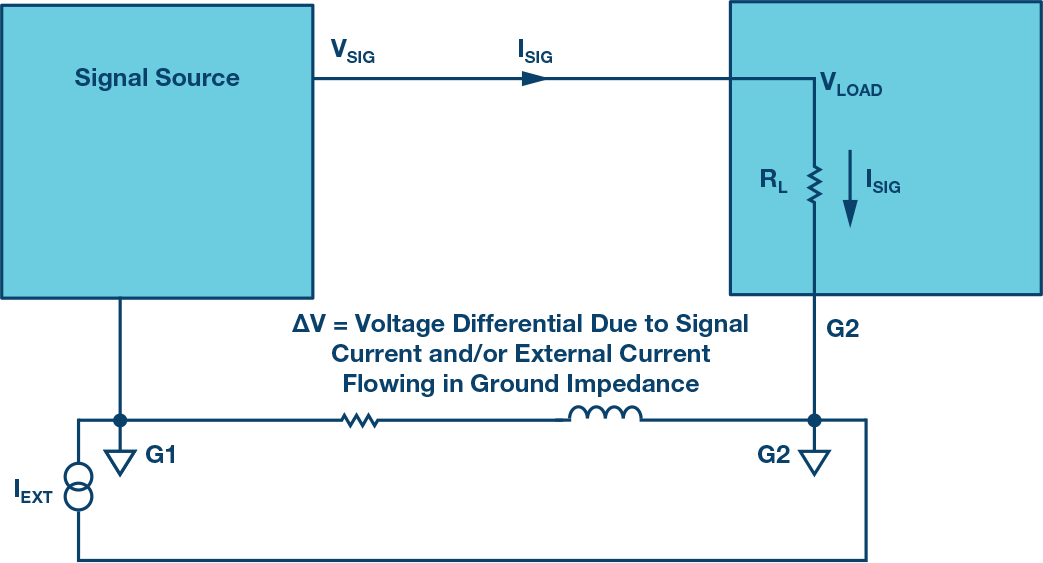
The current flowing between G1 and G2 can be signal current as well as external current due to other circuits.
You can see how the bus impedance in the Figure 1 breadboard will have both resistive and inductive components. Whether or not the ground bus impedance will affect circuit operation depends not only the dc accuracy requirements of the circuit but also the analog signal frequencies as well as the frequency components generated by any digital switching elements in the circuit.
If your maximum signal frequency is 1 MHz, and your circuit only draws a few mA, then the ground bus impedance may not an issue. However, if your signal is 100 MHz, and you are driving a load that requires 100 mA, then the impedance is probably going to be a problem.
In most cases, the use of buss wire is unacceptable as a digital ground return because of its impedance at the equivalent frequency of most logic transitions. For instance, #22 gauge wire has about 20 nH/inch inductance and 1 mΩ/inch resistance. A transient current having a slew rate of 10 mA/ns created by a logic signal transition would develop an unwanted voltage drop of 200 mV at this frequency flowing through 1 inch of this wire:
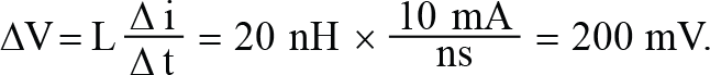
For a signal having a 2 V peak-to-peak range, this translates into an error of about 10% (approximately 3.5-bit accuracy). Even in all-digital circuits, this error would result in considerable degradation of logic noise margins.
For low frequency signals, the 1 mΩ/inch resistance also produces an error. For instance, 100 mA flowing through 1 inch of #22 gauge wire produces a voltage drop of approximately

A signal having a 2 V peak-to-peak range digitized to 16-bit accuracy has a least significant bit (LSB) of 2 V/216 = 30.5 μV. The 100 μV error due to the resistance of the wire therefore becomes approximately 3.3 LSBs of error at the 16-bit level.
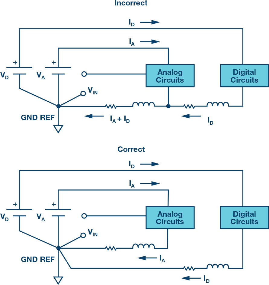
Figure 4 shows how noisy digital currents that flow in the analog ground return path produce errors in the voltage to the analog circuits, VIN. The problem can be mitigated somewhat by connecting the analog and digital circuit grounds together at a single point as shown in the correct lower diagram.
Ground Planes Are Mandatory in Today’s Systems
There is only so much you can do to reduce ground impedance in a solderless breadboard, even one that uses a bus structure as shown in Figure 1. You will rarely find the solderless breadboard used in industrial system designs. A solid ground plane is the industry standard method of providing low impedance current return paths. One or more layers of a production printed circuit board are generally dedicated to ground. This method works well for final production, but is more difficult to implement in prototype systems. Some techniques for incorporating ground planes in prototypes are discussed in the Tutorial MT-100.
Figure 5 shows a typical grounding arrangement for a PCB that contains analog and digital circuits, as well as a mixed-signal device such as an analog-to-digital or digital-to-analog converter.
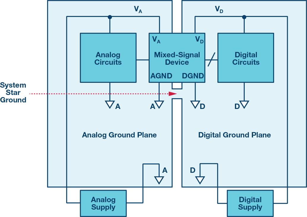
The analog and digital circuits are physically isolated and are placed on their respective ground planes. The mixed-signal device straddles the two ground planes, and the system single-point or star ground is the point at which the two ground planes are connected.
You should understand that there are other grounding philosophies regarding analog and digital grounds that have been proven to work. Some are described in the Tutorial MT-03, which you should refer to for further details. However, the philosophies are all based on the concepts of analyzing the analog and digital current flow paths and then taking steps to minimize their interaction.
So we hope you’ve learned how important grounding is to your current and future designs. In the next installment we will examine the equally important topic of decoupling.
March Quiz Problem
As usual, we end the column with a circuits quiz. Solution in the StudentZone forum on EngineerZone.
References
AN-1142 Application Note, Techniques for High Speed ADC PCB Layout. Analog Devices, Inc., January 2012.
Kester, Walt, James Bryant, and Mike Byrne. Tutorial MT-031, Grounding Data Converters and Solving the Mystery of “AGND” and “DGND.” Analog Devices, Inc., 2009.
Tutorial MT-100, Breadboarding and Prototyping Techniques. Analog Devices, Inc., 2009.
Tutorial MT-101, Decoupling Techniques. Analog Devices, Inc., 2009.
