Understanding the Need for Decoupling Based on Power Supply Rejection Specifications
In the last article, we highlighted the importance of maintaining a low impedance ground plane to provide a path for digital and analog return currents. This article discusses the equally important and related topic of power supply decoupling to maintain low impedances at the points where power enters the integrated circuit (IC).
Analog integrated circuits such as amplifiers and converters have at least two or more power supply pins. In the case of single-supply devices, one of the pins is usually connected to the ground. Mixed-signal devices such as ADCs and DACs can have an analog and digital supply voltage, as well as an I/O voltage. Digital ICs such as FPGAs can also have multiple power supply voltages, such as core voltage, memory voltage, and I/O voltage.
Regardless of the number of power pins, IC data sheets specify allowable ranges on each supply for both recommended operating ranges and absolute maximum values, and these limits must be observed both for proper operation and to prevent damage.
However, small variations in the power supply voltage due to noise or power supply ripple—even if they remain within the recommended operating range—can produce performance degradation in the devices.
In the case of an amplifier, for example, small power supply variations produce small changes in the input and output voltage, as shown in Figure 1.
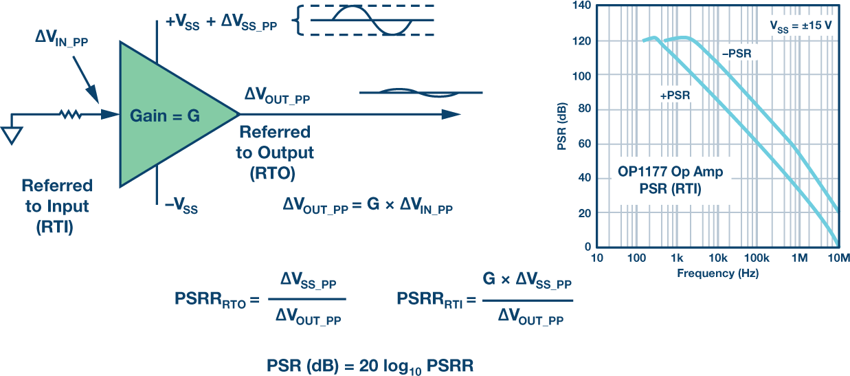
The sensitivity of an amplifier to power supply voltage change is often quantified by the power supply rejection ratio (PSRR) and defined by the ratio of the change in power supply voltage to the change in output voltage. Please refer to Tutorial MT-043 for a more detailed discussion.
Figure 1 shows how the PSR of a typical high performance amplifier (OP1177) degrades with frequency at approximately 6 dB/octave (20 dB/decade). Curves are shown for both the positive and negative supply. Although 120 dB at dc, the PSRR drops rapidly at higher frequencies where more and more unwanted energy on the power line will couple to the output directly.
If the amplifier is driving a load and there is unwanted impedance in the power rails, then the load current modulates the power rails, therefore producing increased noise and distortion in an ac signal.
The performance of data converters and other mixed-signal ICs also degrades with noise on the power supplies, although the actual PSRR may not be given on the data sheet. Power supply noise can also affect digital circuits in a number of ways, including a reduction in logic level noise margins and the introduction of timing errors due to clock jitter.
Proper Localized Decoupling Is Mandatory on the PCB
A typical 4-layer PCB is usually designed with a ground plane layer, power plane layer, and top and bottom signal layers. The ground pins of surface mount ICs connect to the ground plane directly with vias at the pins, thereby minimizing unwanted impedance in the ground connection.
The power supply rail is usually located on the power plane layer and is routed to the various power pins of the ICs. A simple model of an IC showing the power and ground connections is shown in Figure 2.

Currents generated within the IC are shown as the current, IT. The current flowing through the trace impedance, Z, produces a change in the power supply voltage, VS. Depending on the PSR of the IC, this can produce various types of performance degradation as previously discussed.
Sensitivity to power noise and ripple can be minimized by connecting the proper type of localized decoupling capacitor directly between the power pin and the ground plane with a connection that is as short as possible. The decoupling capacitor acts as a charge reservoir to the transient current and shunts it directly to the ground, thereby maintaining a constant power supply voltage on the IC. Although the return current path is through the ground plane, the return current generally doesn’t develop a significant error voltage because of the low ground plane impedance.
Figure 3 shows how the high frequency decoupling capacitor must be as close to the chip as possible. If it is not, the inductance of the connecting trace will have a negative impact on the effectiveness of the decoupling.

Figure 3. Correct and incorrect placement of high frequency decoupling capacitor.
In the left diagram in Figure 3, the connection to both the power pin and the ground are as short as possible, so this would be the most effective configuration. In the right diagram in Figure 3, however, the extra inductance and resistance in the PCB trace will cause a decrease in the effectiveness of the decoupling scheme and may cause interference problems by increasing the enclosed loop.
Selecting the Right Type of Decoupling Capacitors
Low frequency noise decoupling generally requires electrolytic capacitors (typically 1 μF to 100 μF) that act as charge reservoirs to low frequency transient currents. High frequency power supply noise is best reduced with low inductance, surface-mount ceramic capacitors connected directly to the power supply pins of the IC (typically 0.01 μF to 0.1 μF). All decoupling capacitors must connect directly to a low impedance ground plane in order to be effective. Short traces or vias are required for this connection to minimize additional series inductance.
Most IC data sheets show recommended power supply decoupling circuits in the applications section and these recommendations should always be followed in order to ensure proper operation of the device.
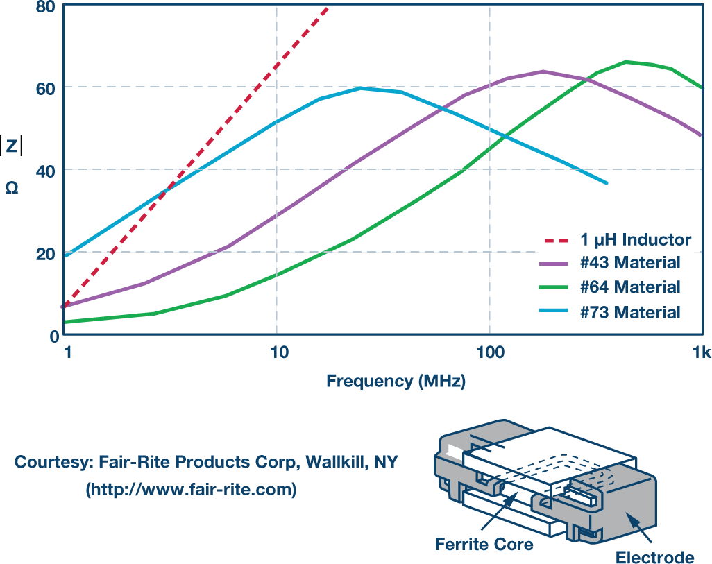
Ferrite beads (nonconductive ceramics manufactured from the oxides of nickel, zinc, manganese, or other compounds) are also useful for decoupling in power supply filters. At low frequencies (<100 kHz), ferrites are inductive—thus they are useful in low-pass LC decoupling filters. Above 100 kHz, ferrites becomes resistive (low Q). Ferrite impedance is a function of material, operating frequency range, dc bias current, number of turns, size, shape, and temperature.
The ferrite beads may not always be necessary, but they will add extra high frequency noise isolation and decoupling, which is often desirable. Possible caveats here would be to verify that the beads never saturate, especially when op amps are driving high output currents. When a ferrite saturates it becomes nonlinear and loses its filtering properties.
Note that some ferrites, even before full saturation occurs, can be nonlinear. Therefore, if a power stage is required to operate with a low distortion output, the ferrite should be checked in a prototype if it is operating near this saturation region. Typical ferrite bead impedances are shown in Figure 4.
The nonideal behavior of capacitors, due to parasitic resistance and inductance, requires careful thought in selecting the proper type for decoupling applications. The discussion of decoupling continues in the next column, where we examine the various types of decoupling capacitors and their applications.
So for now, we conclude the column with the traditional circuit quiz. The solution can be found in StudentZone forum on EngineerZone.®
References
Application Note AN-1142, Techniques for High Speed ADC PCB Layout. Analog Devices, January 2012.
Tutorial MT-100, Breadboarding and Prototyping Techniques. Analog Devices Inc., 2009.
Tutorial MT-101, Decoupling Techniques. Analog Devices, Inc., 2009.
Tutorial MT-031, Grounding Data Converters and Solving the Mystery of “AGND” and “DGND”. Analog Devices, Inc., 2009.
