Introduction
Modern signal processing system design utilizing ADCs, PLLs, and RF transceivers demands lower power consumption and higher system performance. Selecting proper power supplies for those noise sensitive devices is always the pain point for system designers. There is always a trade-off between high efficiency and high performance.
Traditionally, LDO regulators are often used to power those noise sensitive devices. LDO regulators reject the low frequency noise that often presents in system power supplies and they provide clean power to ADCs, PLLs, or RF transceivers. But LDO regulators usually have low efficiency, especially in systems where LDO regulators must regulate down from a power rail several volts above their output voltage. In this kind of situation, LDO regulators typically offer 30% to 50% efficiency, while using switching regulators can reach 90% or even higher efficiency.
Switching regulators are more efficient than LDO regulators, but they are too noisy to directly power ADCs or PLLs without significant performance degradation. One of the noise sources of switching regulators is the output ripple, which can appear as distinct tones or spurs in ADCs output spectrum. To avoid degrading the signal-to-noise ratio (SNR) and spurious-free dynamic range (SFDR), minimizing the output ripple and output noise of switching regulators can be very important.
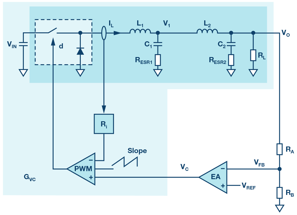
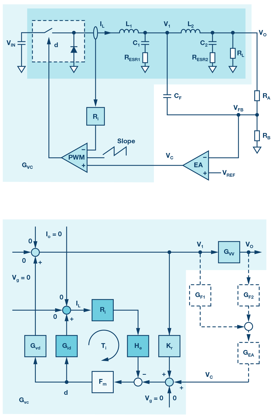
In order to maintain high efficiency and high system performance at the same time, it is often desirable to add a secondary LC filter (L2 and C2) to the output of switching regulator to reduce the ripple and noise, as Figure 1 shows. However, the two-stage LC output filter has associated disadvantages, too. The power stage transfer function is ideally modeled as a fourth-order system that can easily be unstable. If the sample data effect of a current loop1 is also taken into consideration, the complete control-to-output transfer function is shown to be fifth order. An alternate solution is to sense the output voltage from the primary LC filter (L1 and C1) point to stabilize the system. However, applying this approach results in poor output voltage regulation due to the large voltage drops on the secondary LC filter when the load current is heavy, which is not acceptable in some applications.
In this article, a new hybrid feedback method is proposed to provide adequate stability margin and maintain the output accuracy over all the load condition in the application where switching regulators with secondary LC filters are used to provide high efficiency, high performance power supplies to ADCs, PLLs, or RF transceivers.
There has been some published research work on the dc-to-dc converter with a secondary LC output filter.2 – 5 Specifically, the articles “Control Loop Design for Two-Stage DC-to-DC Converters with Low Voltage/High Current Output” and “Comparative Evaluation of Multiloop Control Schemes for a High Bandwidth AC Power Source with a Two-Stage LC Output Filter” discuss the modeling and control of a two-stage voltage-mode converter, which can’t be directly applied to a current-mode converter. A current-mode converter with a secondary LC filter has been analyzed and modeled in “Secondary LC Filter Analysis and Design Techniques for Current-Mode-Controlled Converters” and “Three-Loop Control for Multimodule Converter Systems.” However, both articles have an assumption that the secondary inductor has a much smaller inductance value than the primary inductor, which is not always eligible in real applications.

The outline of this article is as follows:
The small signal modeling of a buck converter with a secondary LC filter is analyzed. A new fifth-order control-to-output transfer function is presented, which is very accurate regardless of the peripheral inductor and capacitor parameters.
A new hybrid feedback method is proposed to provide adequate stability margins while maintaining good dc accuracy of the output voltage. The limitation of the feedback parameters has been analyzed for the first time, which can provide basic criteria for practical design.
Based on the power stage small signal model and new hybrid feedback method, the compensation network is designed. The stability of the closed-loop transfer function is evaluated using a Nyquist plot.
A simple design example is presented based on the power management product ADP5014. With the secondary LC filter, the output noise of ADP5014 in a high frequency range is even better than an LDO regulator.
Appendix Ι and Appendix II present necessary small signal transfer function for power stage and feedback network respectively.
Small Signal Modeling of Power Stage
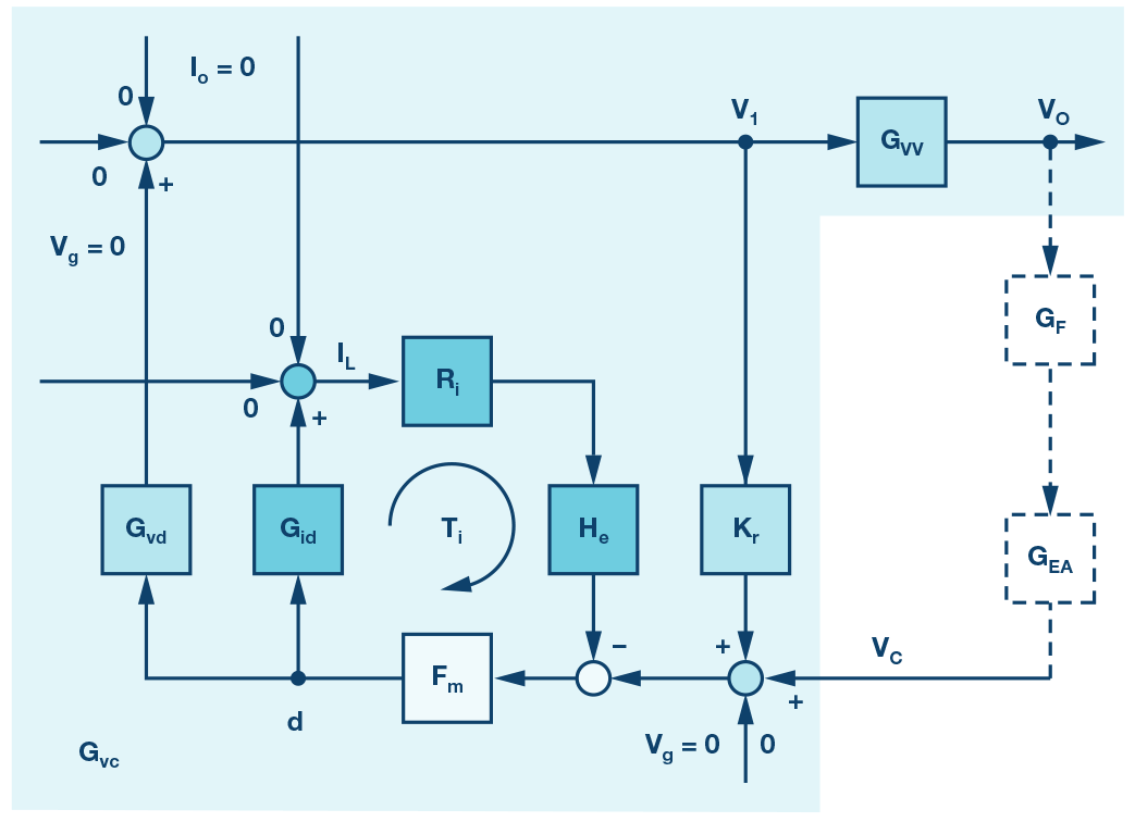
Figure 2 shows the small signal block diagram for Figure 1. The control loop is composed by inner current loop and outer voltage loop. The sample data coefficient He(s) in the current loop refers to the model proposed by Raymond B. Ridley in “A New, Continuous-Time Model for Current-Mode Control.” Note that in the simplified small signal block diagram in Figure 2, the input voltage disturbance and load current disturbance are assumed to be zero since transfer functions related with input voltage and load current will not be discussed in this article.

Buck Converter Example
The new small signal model is demonstrated with a current-mode buck converter with the following parameters:
- Vg = 5 V
- Vo = 2 V
- L1 = 0.8 μH
- L2 = 0.22 μH
- C1 = 47 μF
- C2 = 3× 47 μF
- RESR1 = 2 mΩ
- RESR2 = 2 mΩ
- RL = 1 Ω
- Ri = 0.1 Ω
- Ts = 0.833 μs
Current-Loop Gain
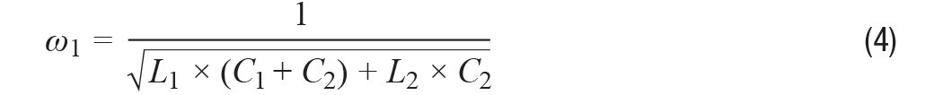
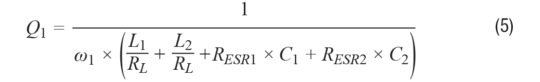
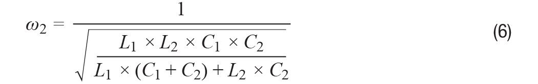
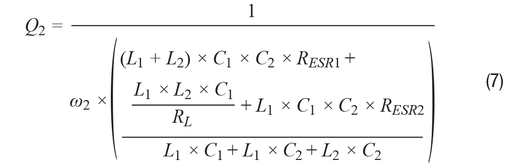
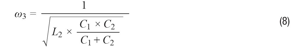
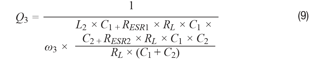
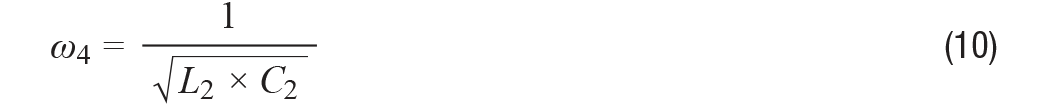
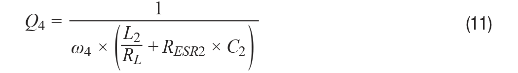
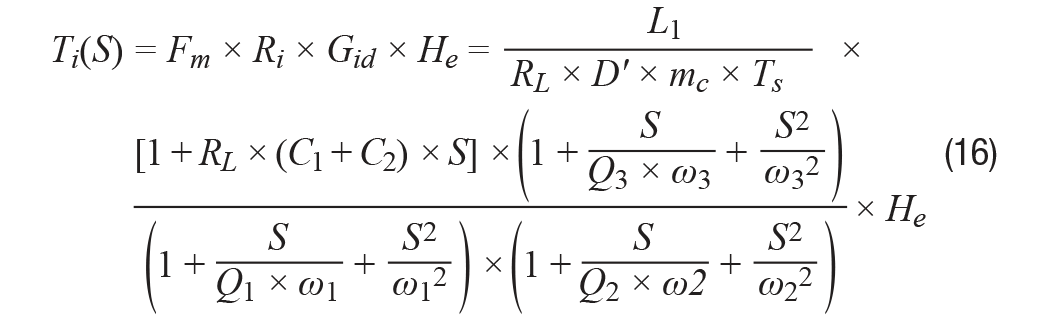
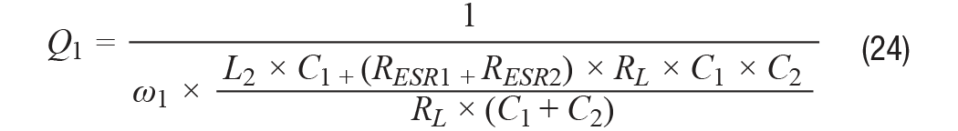
The first transfer function of interest is the current-loop gain measured at the output of the duty-cycle modulator. The resulting current loop transfer function (see Equation 16 in Appendix I) exhibits a fourth-order system with two pairs of complex conjugate poles, which results in two system resonances (ω1 and ω2). Both of these two resonance frequency are determined by L1, L2, C1, and C2. A domain zero is contributed by load resistor RL, C1, and C2. One pair of complex conjugate zeros (ω3) is determined by L2, C1, and C2. Besides, the sample data coefficient He(s) in the current loop will introduce a complex pair of right half plane (RHP) zeros at half of the switching frequency.
Compared with the conventional current-mode buck converter without the secondary LC filter, the new current-loop gain has one more pair of complex conjugate poles and one more pair of complex conjugate zeros, which locate very close to each other.

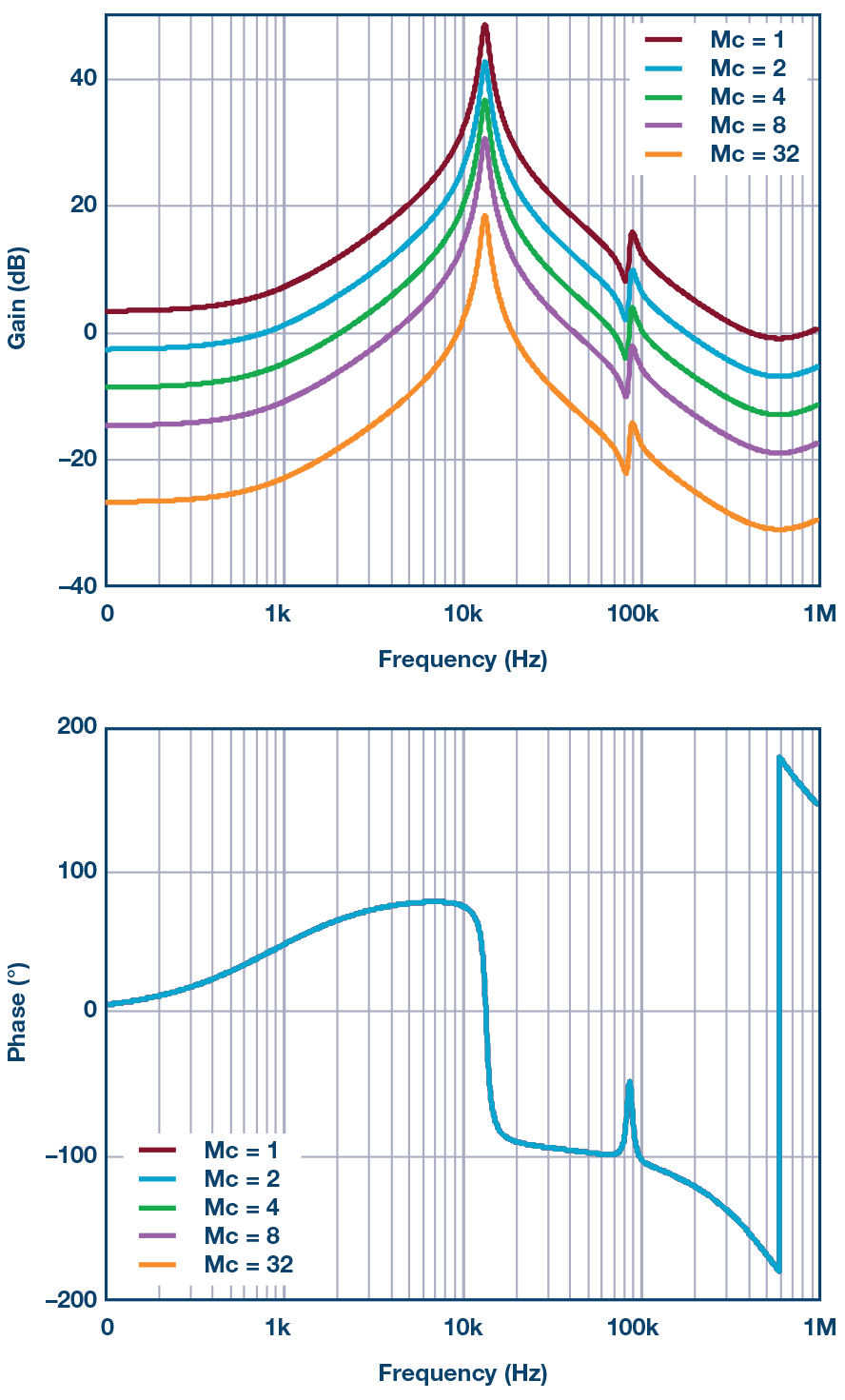
Figure 3 shows a plot of the current-loop gain with different values of external ramp. For the case without external slope compensation (Mc = 1), it can be seen that there is very little phase margin in the current loop, which may lead to subharmonic oscillation. With added external slope compensation, the shape of the gain and phase curves do not change, but the amplitude of the gain will decrease and phase margin will increase.
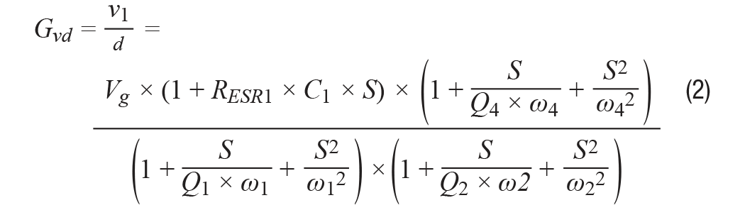
Control-to-Output Gain
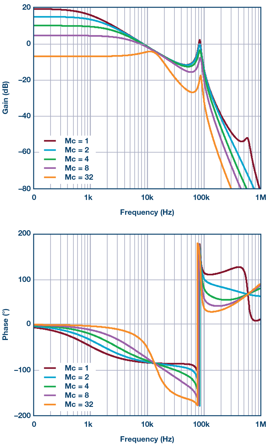
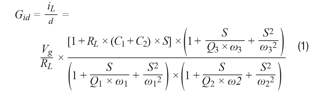
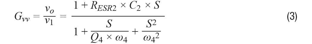
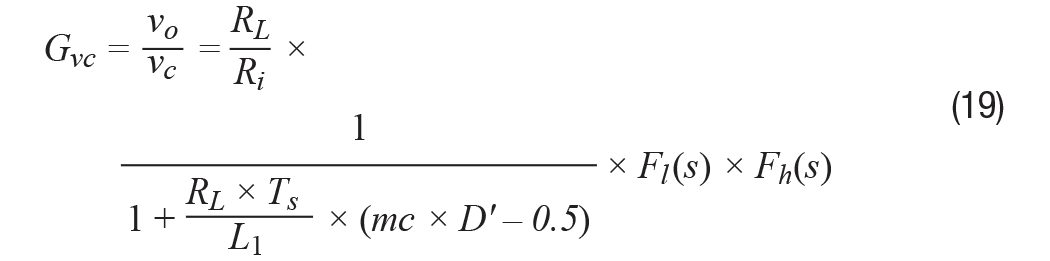
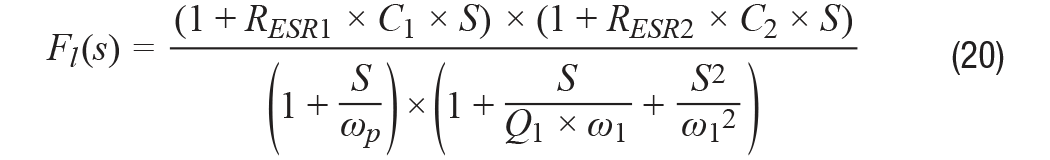
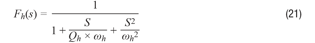
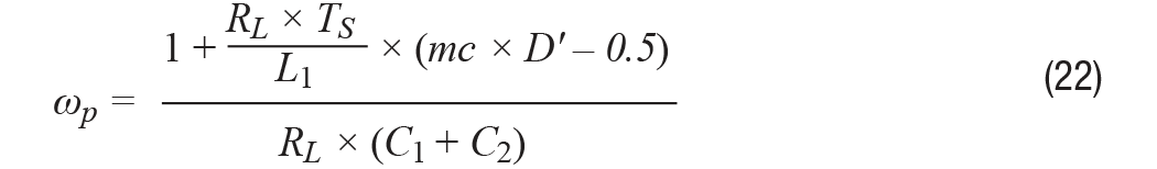
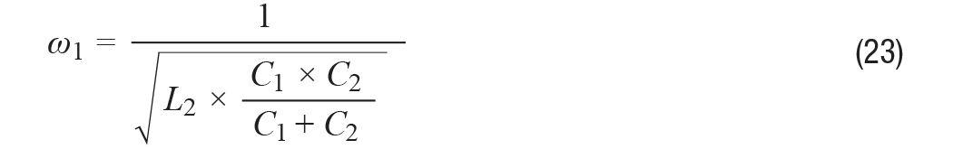
A new control-to-output transfer function is created when the current loop is closed. The resulting control-to-output transfer function (see Equation 19 in Appendix I) exhibits a fifth-order system with one domain pole (ωp) and two pairs of complex conjugate poles (ωl and ωh). The domain pole is mainly determined by load resistor RL, C1, and C2. The lower frequency pair of conjugate poles is determined by L2, C1, and C2, while the higher frequency pair of conjugate poles locate at half of the switching frequency. Additionally, two zeros are contributed by the ESR of C1 and ESR of C2, respectively.
Figure 4 shows a plot of the control-to-output loop gain with different values of external ramp. Compared with the conventional current-mode buck converter, there is one more pair complex conjugate poles (ωl) in the control-to-output gain of current-mode buck converter with a secondary LC filter. The additional resonant poles will give up to 180o additional phase delay. The phase margin drops dramatically, and it can make the system unstable even with Type ΙΙΙ compensation. Besides, Figure 4 clearly shows the transition from current-mode to voltage-mode control as the slope compensation is increased.

The Hybrid Feedback Method
This article presents a new hybrid feedback structure, as Figure 5(a) shows. The idea of hybrid feedback is to stabilize the control loop by using an additional capacitor feedback from the primary LC filter. The outer voltage feedback from the output through resistor divider is defined as the remote voltage feedback and the inner voltage feedback though capacitor CF will be referred to as the local voltage feedback hereafter. The remote feedback and local feedback carry different information on the frequency domain. Specifically, the remote feedback senses the low frequency signal to provide good dc regulation of the output, while the local feedback senses the high frequency signal to provide good ac stability for the system. Figure 5(b) shows the simplified small signal block diagram for Figure 5(a).

The Feedback Network Transfer Function
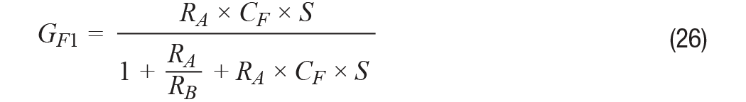
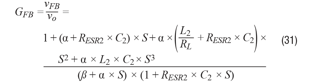
The resulting equivalent transfer function (see Equation 31 and Equation 32 in Appendix II) of a hybrid feedback structure differs significantly from the transfer function of conventional resistor divider feedback. The new hybrid feedback transfer function has more zeros than poles, and the additional zeros will lead to 180o phase ahead at the resonant frequency determined by L2 and C2. Therefore, with the hybrid feedback method, the additional phase delay in control-to-output transfer function will be compensated for by the additional zeros in the feedback transfer function, which will facilitate the compensation design based on the complete control-to-feedback transfer function.
The Limitation of Feedback Parameters
Apart from those parameters in the power stage, there are two more parameters in the feedback transfer function. Parameter β (see Equation 30 in Appendix II) is the output voltage magnification ratio, which is already well-known. However, the parameter α is a brand new concept.
The feedback parameter α (see Equation 29 in Appendix II) can be adjusted to understand the behavior of the feedback transfer function. Figure 6 exhibits the change trend of the zeros in the feedback transfer when α is decreased. It clearly shows that one pair of conjugate zeros will be pushed from left half plane (LHP) to RHP with decreased α.

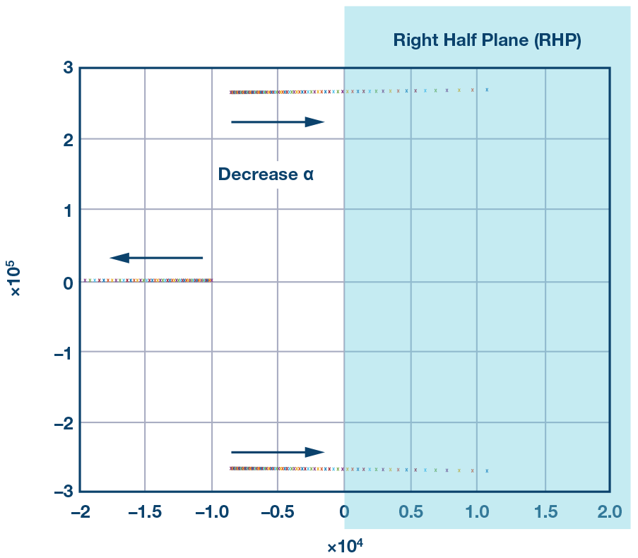
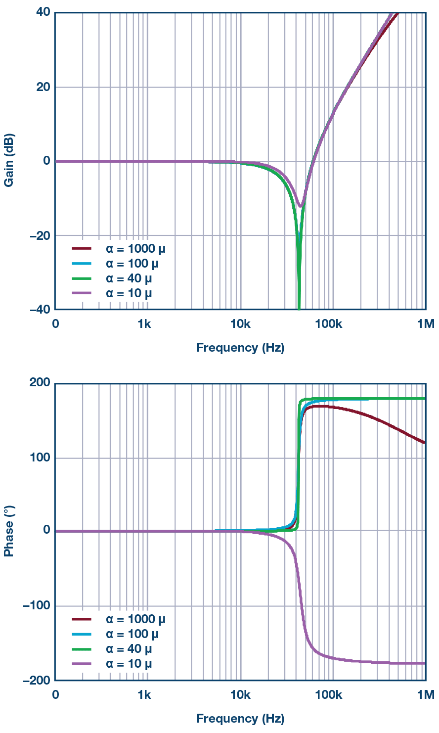
Figure 7 is a plot of the feedback transfer function with a different α. It shows that when α is decreased to 10–6 (for example: RA = 10k, CF = 1 nF), the transfer function of the feedback network will exhibit 180o phase delay, which means the complex zeros have become RHP zeros. The feedback transfer function has been simplified to a new form (see Equation 33 in Appendix II). To keep the zeros in the LHP, the parameter α should always meet the following condition:

Formula 1 gives a minimum limitation basis for feedback parameter α. As long as the condition is satisfied, the control system will be easily stable. However, since RA and CF will work as an RC filter of output voltage change during a load transient, the load transient performance will be degraded with a very big α. So α should not be too large. In practical design, the parameter α is recommended to be 20% to ~30% bigger than the minimum limitation value.

Loop Compensation Design
Design the compensation
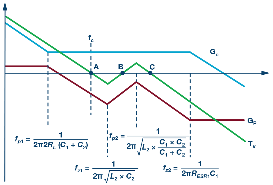
The control-to-feedback transfer function GP(s) can be derived by the product of the control-to-output transfer function Gvc(s) and the feedback transfer function GFB(s). The compensation transfer function GC(s) is designed to have one zero and one pole. The asymptotic Bode plots of the control-to-feedback and compensation transfer function, as well as closed-loop transfer function TV(s), are shown in Figure 8. The following procedures show how to design the compensation transfer function.
Determine the cross frequency (fc). Since the bandwidth is limit by fz1, choosing an fc smaller than fz1 is recommended
Calculate the gain of GP(s) at fc, then the middle frequency band gain of GC(s) should be the opposite number of GP(s)
Place the compensation zero at the domain pole (fp1) of the power stage
Place the compensation pole at the zero (fz2) caused by the ESR of output capacitor C1.

Using a Nyquist Plot to Analyze Stability
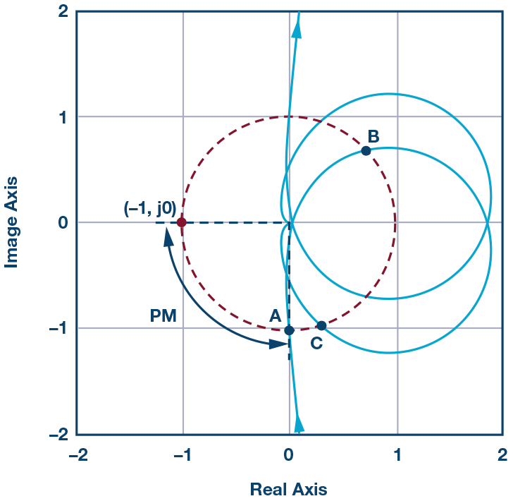
According to Figure 8, the closed-loop transfer function TV(s) has crossed 0 dB three times. The Nyquist plot is used to analyze the stability of closed-loop transfer function, as Figure 9 shows. Since the plot is far away from (–1, j0), the closed loop is stable and has adequate phase margin. Note that the points A, B, and C in the Nyquist plot correspond to the points A, B, and C in the Bode plot.

Design Example
The ADP5014 optimizes many analog blocks to achieve lower output noise at a low frequency range. The unit-gain voltage reference structure also makes its output noise independent from the output voltage setting when VOUT setting is less than the VREF voltage. A secondary LC filter is added to attenuate the output noise at a high frequency range, especially for fundamental switching ripple and its harmonic. Figure 10 shows the design details.

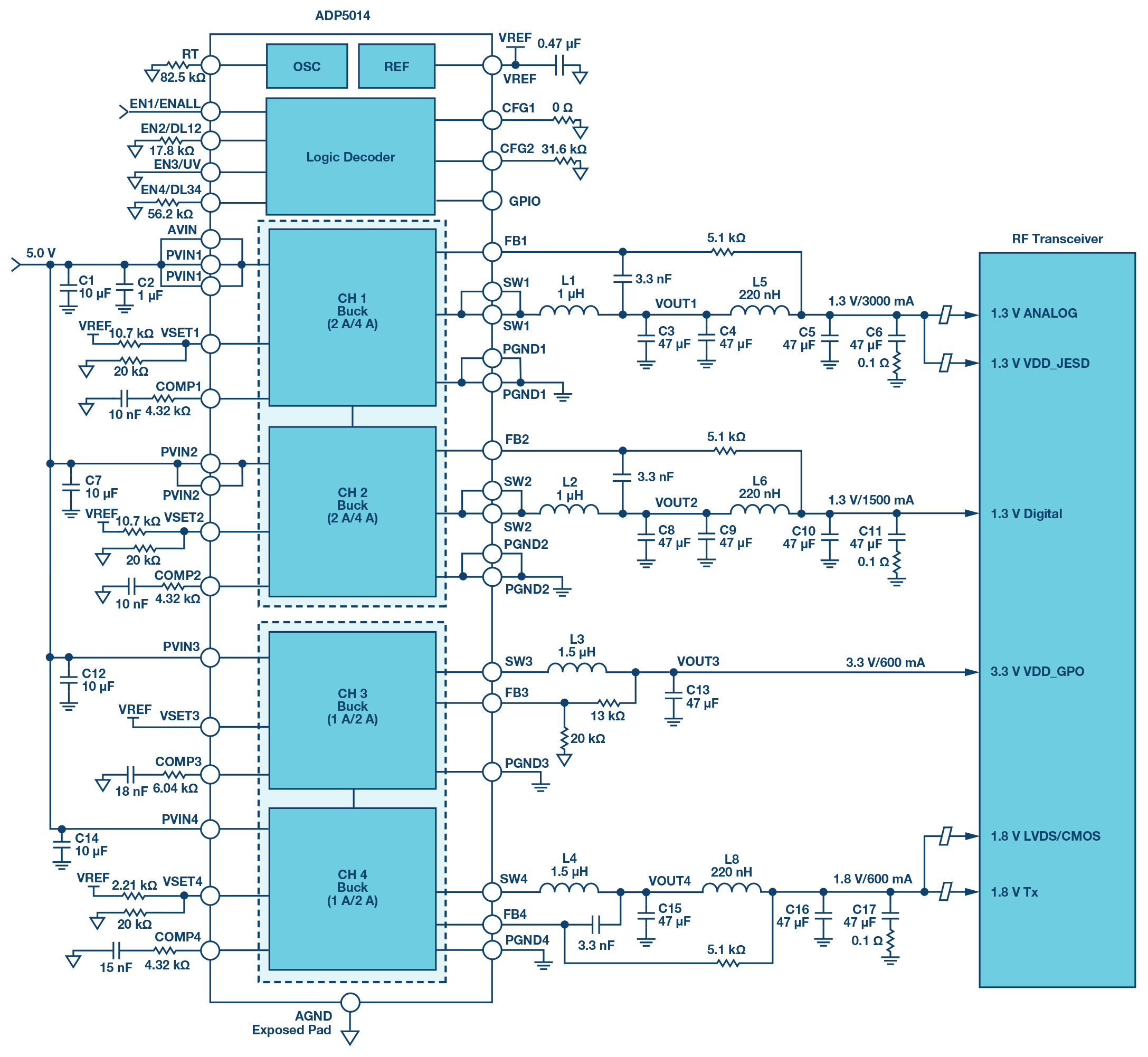
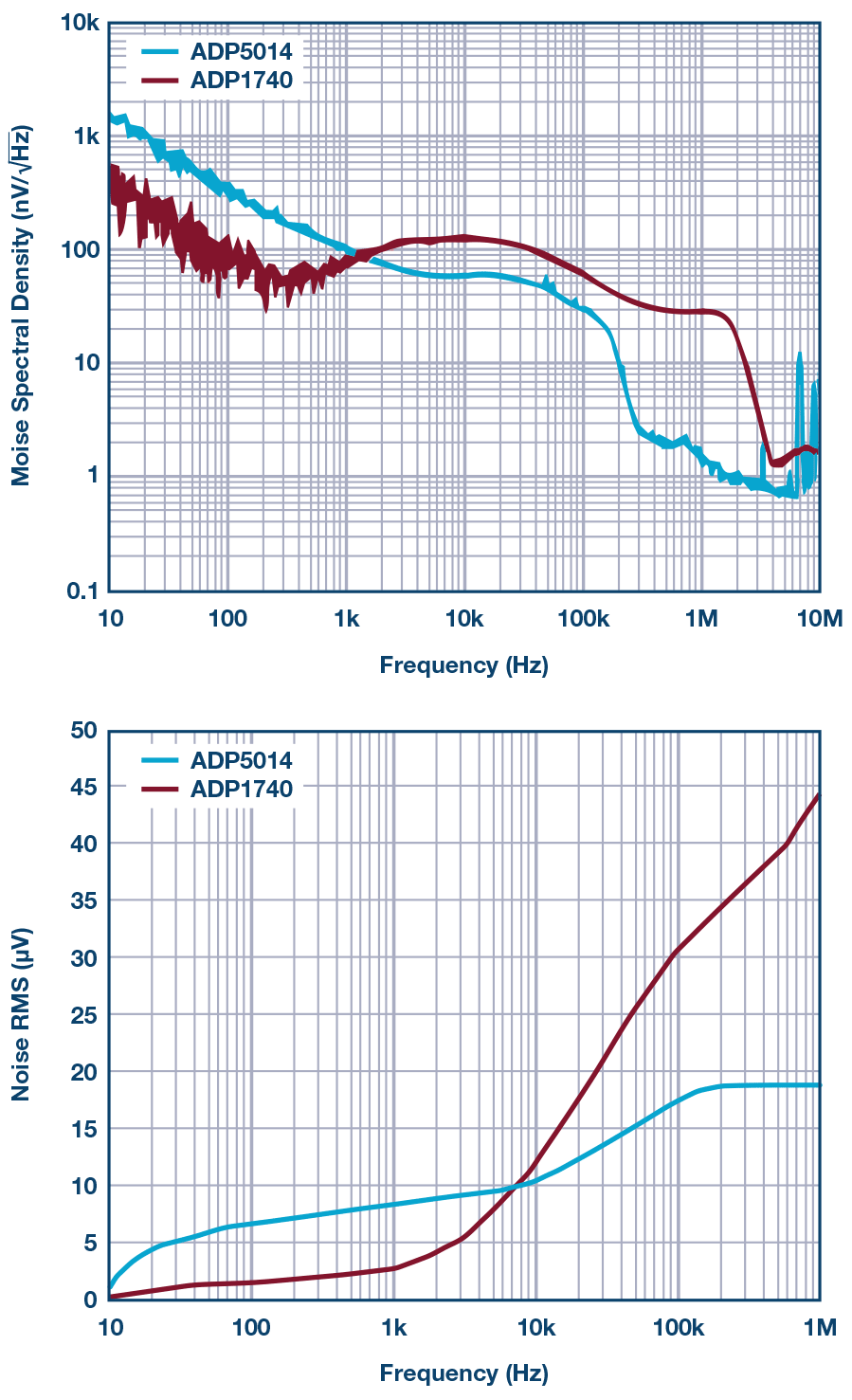
Figure 11 shows the ADP5014 noise spectral density measurement from a 10 Hz to 10 MHz frequency range and integrated rms noise from a 10 Hz to 1 MHz frequency range, compared to the ADP1740s as another traditional, 2 A, low noise LDO regulator. The output noise of ADP5014 in the high frequency range is even better than ADP1740’s.

Conclusion
This article presents a general analysis framework for modeling and control for a current-mode buck converter with a secondary-stage LC output filter. The accurate control-to-output transfer function is discussed. A new hybrid feedback structure is proposed and the feedback parameter limitation is deduced.
The design example shows that a switching regulator with secondary LC filter and hybrid feedback method can provide a clean, stable power supply that is competitive with, or even better than, an LDO regulator.
Modeling and control in this article concentrates on a current-mode buck converter, but the methods described here can be applied to voltage-mode buck converters as well.
Appendix Ι
The power stage transfer functions in Figure 2 are as follows.
where:
where: L1 is the primary inductance.
C1 is the primary capacitance.
RESR1 is the equivalent series resistance of the primary capacitor.
L2 is the secondary inductance.
C2 is the secondary capacitance.
RESR2 is the equivalent series resistance of the secondary capacitor. RL is the load resistance.
The gain blocks in the current loop are as follows.


where:


where: Ri is the equivalent current sense resistance
Se is the sawtooth ramp of slope compensation
Sn is on-time slope of the current sense waveform
Ts is the switching period
The current-loop gain is
where:

where:
D is the duty cycle
According to Figure 2, the gain block kr is given by

The control-to-output transfer function is
where:

Appendix ΙΙ
In Figure 5, the local feedback and remote feedback transfer function are
According to Equation 1 through Equation 27, the control-to-feedback transfer function is given by
where:


where: RA is the top resistor of feedback resistor divider
RB is the bottom resistor of feedback resistor divider
CF is the local feedback capacitor
The equivalent feedback network transfer function is
The approximate feedback transfer function is

where:

In typical low noise applications, the unit-gain voltage reference structure is usually applied, so parameter β will be equal to 1. Then the feedback transfer function is

References
1Raymond B. Ridley. “A New, Continuous-Time Model for Current-Mode Control.” IEEE Transactions on Power Electronics, Vol. 6, No. 2, 1991.
2Julie Yixuan Zhu and Brad Lehman. “Control Loop Design for Two-Stage DC-to-DC Converters with Low Voltage/High Current Output.” IEEE Transactions on Power Electronics, Vol 20, No. 1, 2005.
3Patricio Cortes, David O. Boillat, Hans Ertl, and Johann W. Kolar. “Comparative Evaluation of Multiloop Control Schemes for a High Bandwidth AC Power Source with a Two-Stage LC Output Filter.” International Conference on Renewable Energy Research and Applications, IEEE, 2013.
4Raymond B. Ridley. “Secondary LC Filter Analysis and Design Techniques for Current-Mode-Controlled Converters.” IEEE Transactions on Power Electronics, Vol. 3, No. 4, 1988.
5Byungcho Choi, Bo H. Ch, Fred C. Lee, and Raymond B. Ridley. “Three-Loop Control for Multimodule Converter Systems.” Power Electronics IEEE Transactions on Power Electronics, Vol. 8, No. 4, 1993.
