Reliable PCB Assembly of Land Grid Array Packages in Planar Phased Array Antennas
Reliable PCB Assembly of Land Grid Array Packages in Planar Phased Array Antennas
2021-12-01
Introduction
High frequency planar phased arrays often require a complexity from their beamforming ICs and transmit/receive (T/R) modules that force the devices into high pin-count land grid array (LGA) packages, so that all the RF circuits fit into a λ/2 lattice spacing. LGA packages have recessed pins located on their bottom side. As a result, PCB solder mask variation and solder volume invariance both contribute to difficult PCB assembly if the LGA footprint is not designed correctly. This article gives guidelines for proper LGA footprint design that leads to high yield PCB assembly and gives a practical LGA footprint design example using the large, high pin-count ADAR1000 beamformer IC.
Planar Phased Array Systems
Phased array technology uses an arrangement of antenna elements where the relative phase of each element is varied to steer the focused radiation pattern, also known as a beam. The beam can be aimed in various directions electronically, overcoming the limited speed and reliability problems of a mechanically steered antenna. A phased array system significantly reduces size, weight, and power (SWaP), making it an attractive technology for defense applications such as radar, communications, space, and electronic warfare.
In addition to eliminating moving mechanical parts, implementing a flat panel radar front end—where patch antennas and RF electronics populate the opposite sides of the same PCB—has obvious appeal as a size reducer. For analog and hybrid (analog/digital) beamforming systems, the 4-channel beamformer has become the form factor of choice. This arrangement consists of a series of cells with the quad beamformer at the center surrounded by four T/R modules (see Figure 1).

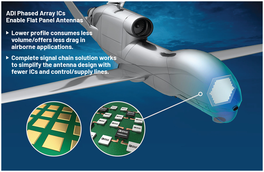
Figure 1. A planar phased array front end with electronics and patch antenna elements on opposite sides of the same printed circuit board (PCB).
The multichannel functionality of these beamformers along with support and control circuitry (for example, receiver and transmitter RF traces, amplifier bias control lines, and T/R control lines between the beamformer and the T/R module) forces the beamformer ICs into high pin-count packages. This migration is also driven by the need to conform to a lattice spacing of lambda over two (15 mm at 10 GHz). As a result, LGA packages have become a popular choice for multichannel beamformer ICs. The ADAR1000 shown in Figure 2 is a prime example of a typical beamformer IC in an LGA package.


Figure 2. A typical LGA package with a high pin count and dual rings of pins.
The Soldering Process
Automated PCB assembly is a multistep process. It begins with the application of solder paste to the exposed metal on the PCB. This is done by placing a solder stencil on top of the PCB and aligning the holes in the solder stencil with the exposed PCB metal underneath. Solder paste is then applied. The stencil is then removed, and the surface-mount components are placed on the board, resting on the deposited solder paste. The board, solder paste, and components are then placed in a reflow oven, where the solder paste melts and bonds to the PCB and the pads of the components. In this process there are multiple variables at play, which can lead to problems.
Solder Mask Variance and Stencil Invariance
Along with the solder stencil, the solder mask on the PCB (which usually has a familiar green color) defines where solder paste should be applied to the PCB. A popular design approach involves making the solder mask openings (apertures) slightly smaller than the metal pads underneath (so-called solder mask defined pads).
Many PCBs use liquid photo-imageable (LPI) solder masks that meet the IPC-SM-840 Class 3 standard. Depending on the fabrication lot, vendor, etc., the solder mask apertures can vary in size and be misaligned due to solder mask registration errors. An example of a solder mask with varying apertures is shown in Figure 3 (highlighted with red rectangles).

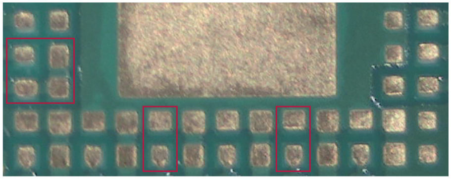
Figure 3. Examples (in red rectangles) of neighboring LGA pads having solder mask variation.
Where pads are solder mask defined and where there is aperture-to-aperture variation, the effective size of the exposed copper pad will vary even though the copper pad itself it not varying. This is especially true when there are large sections of copper, usually connected to ground, beneath the solder mask.
Let’s focus next on the metal solder stencil. Variations in the size of openings in a solder stencil can result in varying amounts of solder paste being applied to each pad. However, because solder stencils are generally laser cut from stainless steel sheets by machines capable of minimum cut widths of 0.05 mm or better and aperture tolerances of 0.013 mm or better, the practical variance from opening to opening is very small. These tight tolerances ensure uniform volume of solder paste being deposited onto the exposed copper of the PCB. An example of a solder stencil is shown in Figure 4.


Figure 4. Example of a solder stencil.
The combination of the solder mask size variations and solder stencils with little or no size variation can set up a situation in which PCB assembly is not reliable due to pin-to-pin shorts and/or pin opens.
Open circuits can be caused by a single PCB pad having a larger aperture size while neighboring pads have nominal or smaller than nominal apertures. Figure 5a shows an exaggerated side view of an LGA package sitting on a PCB after solder paste has been applied. When the solder paste heats up, the solder ball that forms in the well that results from the solder mask opening, stands high enough to bond to the recessed pin. Figure 5b illustrates a case where the solder mask opening is larger than normal. Here again, a solder ball forms inside the well. However, because the opening is larger, the height of the solder ball is reduced and does not bond to the recessed pin.

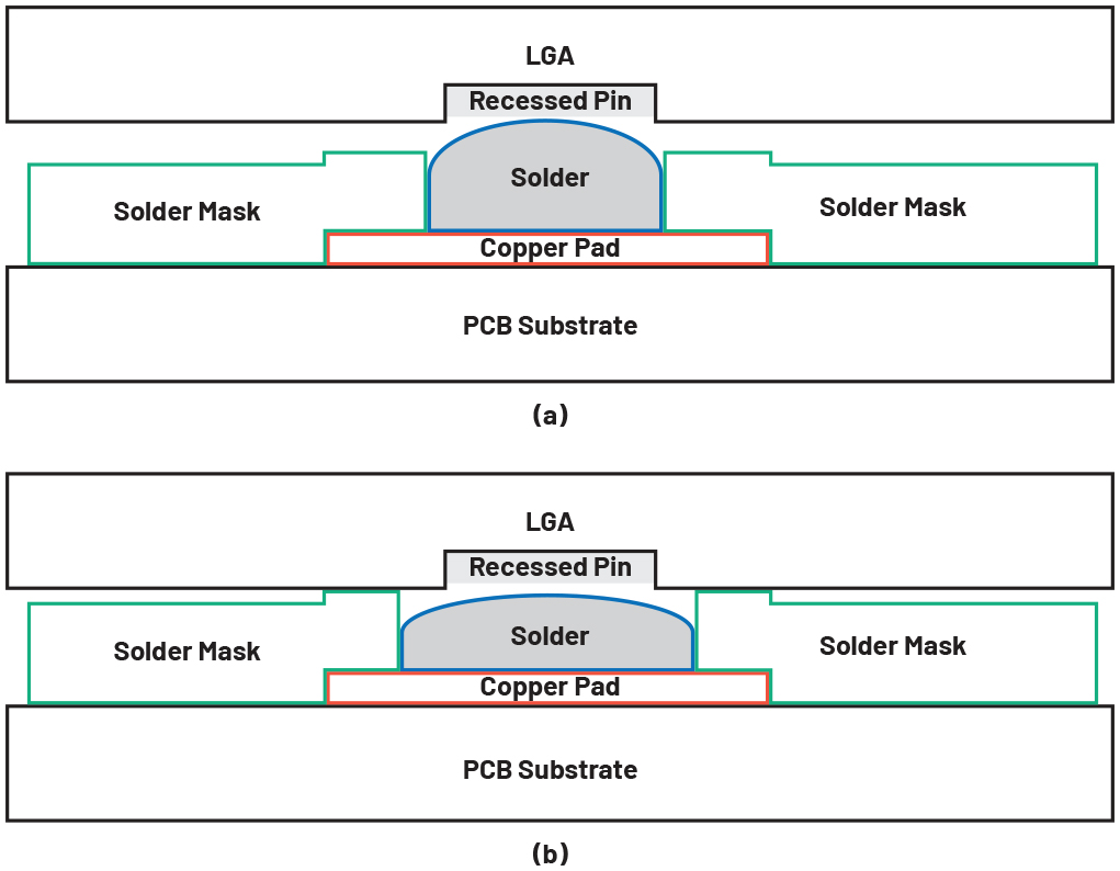
Figure 5. Side view of a pin-to-solder-to-pad interface where (a) a nominal solder mask aperture size creates a proper connection to the pin and (b) a larger than nominal aperture causes a pin open (not to scale; dimensions exaggerated for illustration purpose).
PCB Footprint Design Guidelines
With the goal of minimizing the effects of PCB and package variance, the following guidelines are recommended for reliable LGA PCB assembly. These guidelines are applicable to LGA packages with pins of dimensions 0.25 mm (square or rectangular), and with 0.5 mm pitch, and similar geometries.
- PCB pads should be 20% larger in each direction relative to the nominal LGA package pin dimensions, as shown in Figure 6. This ends up being approximately 0.05 mm larger for packages with 0.25 mm square pins.
- Oversizing the pad helps reduce the effects of registration errors.

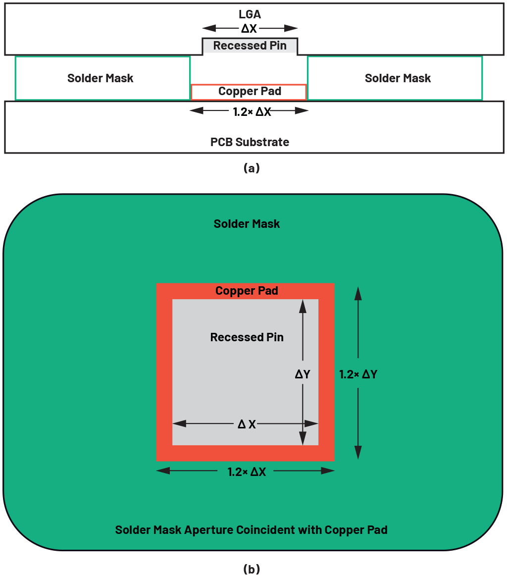
Figure 6. (a) Side view and (b) top view of oversized PCB pad and solder mask relative to IC pad size.
- The PCB pad to solder mask opening should be a 1:1 ratio. This is neither a solder mask defined nor a non-solder mask defined solution, but rather a hybrid solution.
- Keeping the 1:1 ratio helps with having both enough solder for proper connectivity and sufficient solder dam between the pads to help prevent shorts.
- On the paste mask/solder stencil, break up the ground paddle opening into several smaller openings, such that they are similar in size to the pins on the part.
- This evenly distributes solder over the large exposed copper sections of the PCB.
- Remove the silkscreen LGA outline.
- This removes any possibility of the outline affecting the planarity of the LGA.
- Remove any silkscreen outline of components that are near the LGA.
- Move any silkscreen text, Pin 1 designators, etc. away from the LGA.
- A 1.85 mm keep-out region from the nearest device pad is recommended.
- Move components as far away as possible from the LGA.
- A 2.3 mm keep-out region from the nearest device pad is recommended.
Note: these last three guidelines affect the assembly less than the first four guidelines and fall into the best practices category. Nonetheless, it’s still recommended that they be implemented where possible and to a degree that PCB space allows.
While packages with smaller pin and pitch geometries are beyond the scope of this article, these guidelines should still be applicable, at least as a starting point for the footprint design. Advanced board design and fabrication techniques may need to be used to account for the solder mask variation when using appreciably smaller pad and pitch geometries.
Design Example: ADAR1000 PCB Footprint
The following details the design of the footprint for the ADAR1000, an 8 GHz to 16 GHz, 4-channel, X-band and Ku-band beamformer intended for planar phased array applications. This footprint design is used on the ADAR1000-EVALZ evaluation board.
ADAR1000 Package Outline Drawing
The ADAR1000 is in a 7 mm × 7 mm LGA package, which has an inner and outer ring of pins and an exposed ground paddle in the center. Each pin is nominally 0.25 mm square, with variation of ±0.05 mm. The nominal exposed ground paddle dimensions are 4.25 mm × 3.25 mm. The remaining dimensions of the bottom side of the package are shown in Figure 7. Not shown is the pin recess depth, which is 0.02 mm from bottom of package to pin.

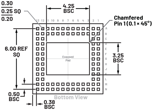
Figure 7. ADAR1000 package outline drawing (bottom view); dimensions shown in millimeters.
ADAR1000 Recommended PCB Footprint Design
Applying the guidelines for reliable assembly, the following was done to the ADAR1000 PCB footprint:
- The PCB pads were oversized by 20%, which is 0.05 mm larger than the nominal size of the ADAR1000 pins. This makes the pad size 0.3 mm × 0.3 mm. This is shown in Figure 8.

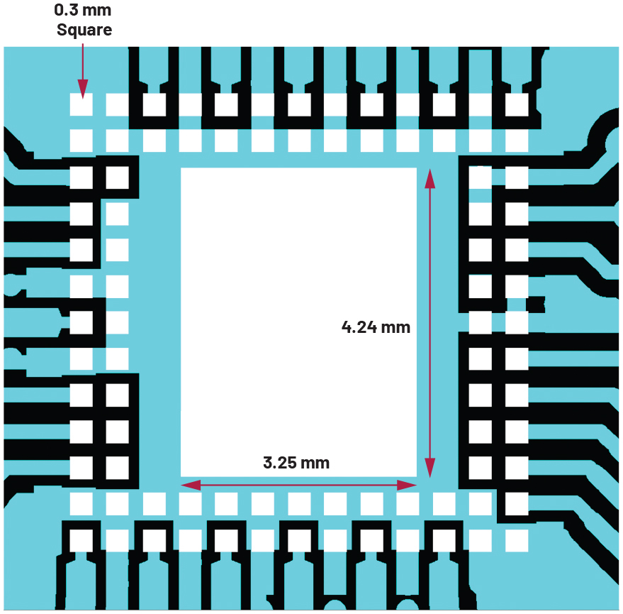
Figure 8. ADAR1000 PCB recommended footprint with 0.3 mm × 0.3 mm pads highlighted in white. The rest of the layer 1 metal is shown in aqua.
- The solder mask aperture dimension was set equal to that of the PCB pads, which is 0.3 mm × 0.3 mm. This is shown in Figure 9.

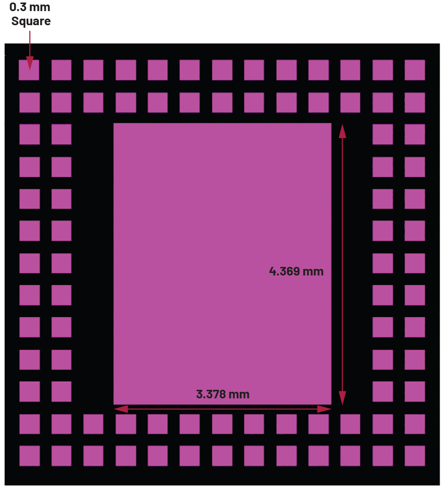
Figure 9. ADAR1000 solder mask with 0.3 mm × 0.3 mm pad openings and 3.378 mm × 4.369 mm ground paddle opening.
- The solder stencil was designed such that the ground paddle opening is broken up into smaller apertures that are similar in size to the pins of the LGA. The pin apertures were set to 0.28 mm square, while the ground paddle apertures were set to 0.406 mm × 0.28 mm. The solder stencil design is shown in Figure 10.
- Figure 11 shows a picture of wet solder paste deposited from a stencil with the ground paddle opening broken up into several smaller apertures.

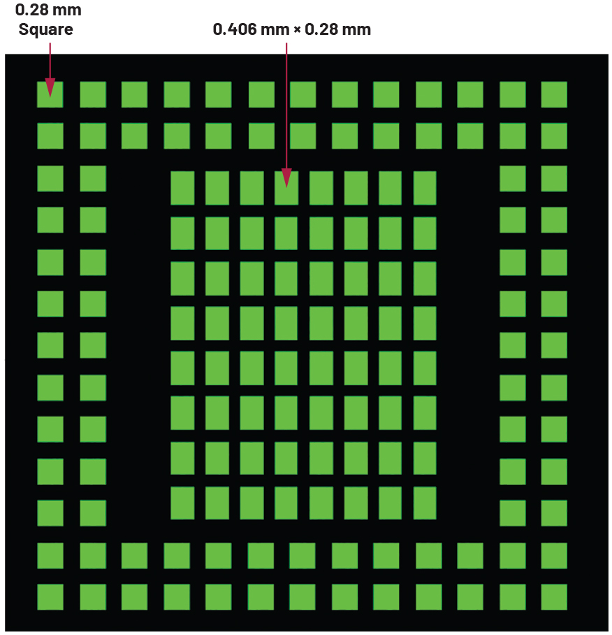
Figure 10. ADAR1000 PCB paste mask (solder stencil) with 0.28 mm × 0.28 mm pad openings and 0.406 mm × 0.28 mm ground paddle openings.

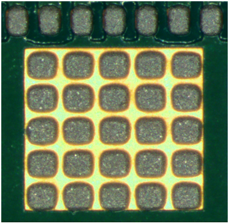
Figure 11. Example of wet solder paste (prior to reflow) on a copper ground pad that has been deposited by a solder stencil with multiple smaller apertures for the ground pad. Signal pins are shown at the top of the picture for reference.
- The silkscreen outline around the ADAR1000 was removed.
- The silkscreen outlines around the components that are within 2.3 mm from the ADAR1000 were removed.
- Any silkscreen text or features near the ADAR1000, such as a Pin 1 designator, were moved away from the ADAR1000 to the recommended distance of 1.85 mm.
- The closest component was set to 2.3 mm from the ADAR1000.
The last four guidelines are illustrated in Figure 12 and Figure 13. As can be seen in Figure 12:
- There is no ADAR1000 silkscreen outline.
- The nearest component (C21) is 2.3 mm away.
- The nearest silkscreen feature (C21 outline) is 1.85 mm away. The next nearest silkscreen feature is the C35 text.

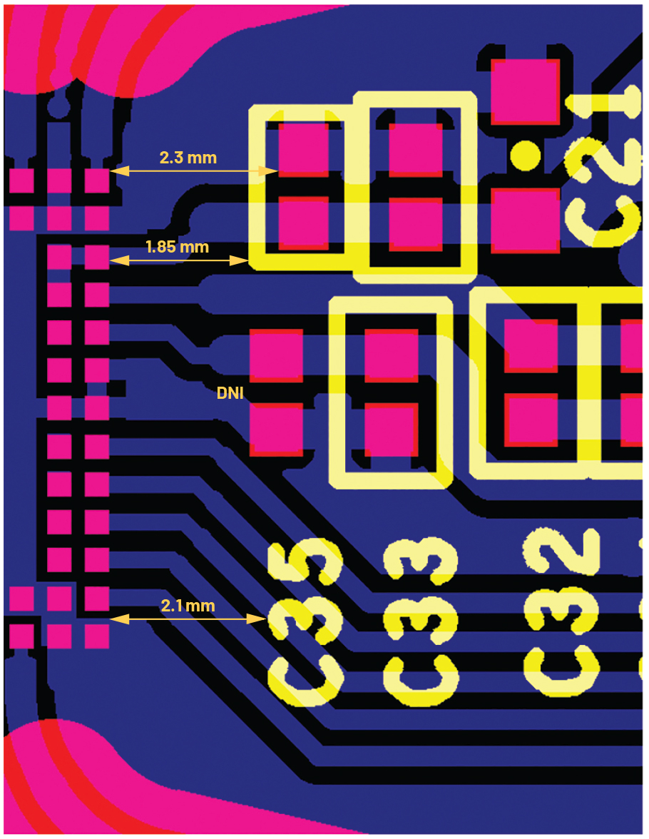
Figure 12. ADAR1000 PCB keep-out regions; silkscreen features are at a minimum of 1.85 mm from DUT pads; the nearest populated component is 2.3 mm from DUT pads.

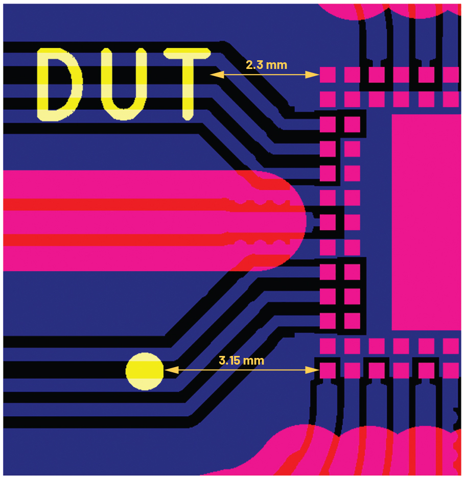
Figure 13. ADAR1000 PCB keep-out regions; silkscreen features are at a minimum of 1.85 mm from DUT pads.
Shown in Figure 13, both the DUT silkscreen text and the Pin 1 designator were moved well outside the 1.85 mm keep-out region. For the ADAR1000, this minimum keep-out region is 1.795 mm from the edge of package. If the distance between package edge and pin edge is large, it is recommended to reference the keep-out regions to the package edge, instead of the pin edge as shown in this article.
The ADAR1000 evaluation board allowed for keeping the nearest components and silkscreen features well away from the ADAR1000. This keep-out region is not always possible on planar phased array application boards, but board designers should keep this guideline in mind when designing their board and observe these guidelines as best as possible.
Conclusion
While LGA packages offer the high pin-count density that is required in high frequency planar phased array electronics with antenna element spacing set to λ/2, successfully soldering them to a PCB can be challenging. The main guidelines discussed in this article of 1) increasing the PCB pad size by 20% larger than the LGA pins, 2) setting the solder mask aperture to be the same size as the PCB pads, and 3) designing the solder stencil such that the ground paddle opening is broken up into smaller apertures that are similar in size to the pins of the LGA, all contribute to reducing the effect of PCB manufacturing variances. These guidelines have been proven to deliver a high yield board assembly consistently across manufacturing and assembly lots. Having reliable assembly prevents the need for any PCB rework, which saves money and decreases time to market.
关于作者
{{modalTitle}}
{{modalDescription}}
{{dropdownTitle}}
- {{defaultSelectedText}} {{#each projectNames}}
- {{name}} {{/each}} {{#if newProjectText}}
-
 {{newProjectText}}
{{/if}}
{{newProjectText}}
{{/if}}
{{newProjectTitle}}
{{projectNameErrorText}}
最新视频 21


