Power Supply Subsystems for Photoplethysmography Remote Patient Vital Sign Monitors—Part 2
Power Supply Subsystems for Photoplethysmography Remote Patient Vital Sign Monitors—Part 2
2024-12-19
Read other articles in this series.
摘要
This two-part article presents validated switch-mode power circuit designs for remote patient monitoring applications, including biosensors with excellent system signal-to-noise performance. “Power Supply Subsystems for Photoplethysmography Remote Patient Vital Sign Monitors—Part 1“ presents a discrete solution for best performance and “Power Supply Subsystems for Photoplethysmography Remote Patient Vital Sign Monitors—Part 2“ features an integrated solution for space-constrained applications.
- Learn how to select a power supply configuration based on photoplethysmogram (PPG) system requirements.
- Review the implementation of switch-mode power supply reference circuits for both discrete (Part 1) and integrated designs (Part 2).
- See a power supply performance test methodology that validates the system over different device use cases and transient loading conditions.
- Get a checklist to validate the implementation.
- Gain troubleshooting knowledge to address implementation issues.
Introduction
This two-part article presents prevalidated power supply circuit designs for PPG remote patient vital sign monitoring applications, including biosensors with excellent system signal-to-noise performance. A PPG device can be implemented to measure blood volume changes from which vital sign information such as blood oxygen levels and heart rates are derived. In Part 1, we provided discrete power supply circuit design solutions for best performance using the MAX86171 optical pulse oximeter and heart-rate sensor analog front end (AFE). In Part 2, we now show an integrated solution for space-constrained applications using the MAX86141 optical pulse oximeter and heart-rate sensor AFE (can be used with the MAX86171 as well).
As mentioned in Part 1 of this article, Analog Devices simplifies and speeds the development process by offering power supply subsystem circuit designs that have been prevalidated (that is, designed, built, and tested) ensuring the signal-to-noise ratio (SNR) performance of each biosensing AFE device. We provided a discrete option in Part 1 and now we will provide an integrated solution.
To reiterate, below are details for the power supply circuits with each example being complemented with a validation checklist and troubleshooting guide to aid circuit designers if needed. Here, Figure 1 shows a standard power block diagram encountered in many remote patient monitoring applications.


| Input | Output (VDIG, VANA, VLED) | Noise, RTO | ||
| VIMIN | VIMAX | VOMIN | VOMAX | Vp-p(max) |
| 3.0 V1 | 4.2 V1 | 1.6 V | 2.0 V | 30 mV p-p |
| 2.0 V2 | 3.4 V2 | 1.6 V | 2.0 V | 30 mV p-p |
| 4.7 V | 5.3 V | 20 mV p-p | ||
Note:
1Secondary cell battery (LiPo)
2Primary cell battery (Li coin cell)
| Design Configuration | Battery Implementation | Board Area Layout Considerations |
| Discrete | Primary (coin cell) Secondary (Li and LiPo) | Implements separate discrete circuits |
| Integrated | Secondary (Li and LiPo) | Uses single integrated circuit for minimal board area requirements
Supports secondary batteries only |
Integrated Design Description
This DC-to-DC power management integrated circuit (PMIC) design is used to regulate three output power supply rails for use in a remote patient vital sign monitor subsystem. The IC features a single-inductor multiple-output (SIMO) buck-boost regulator that provides the power rails from a single inductor to minimize total solution size while maintaining high efficiency.
This circuit provides proper line and load regulation while maintaining low output noise levels needed to preserve biosensor SNR performance, which is powered by a rechargeable lithium polymer battery. Figure 2 shows the PPG subsystem using an integrated power supply device.


| Designator | Component | Description |
| U1 | DC-to-DC converter | Power converter device (MAX77642) |
| L1 | 2.2 μH inductor | Low equivalent series resistance (ESR) inductor (energy) storage component1 |
| C1 | 22 μF capacitor | Low ESR capacitor (energy) storage component1 |
1L1 and C1 are specially selected passive components that are critical to the performance of the DC-to-DC converter (also known as, switch-mode power supply).
1.8 V/1.8 V/5.0 V SMPS Circuit Using a PMIC
The following circuit based on the MAX77642 PMIC shows typical input and output power supply levels for a properly operating SMPS device in remote patient vital sign monitor applications. As shown in Figure 3, a digital multimeter (DMM) can be used to probe the input and output ports to validate the supply voltage levels. The power supply output levels can vary due to several factors such as:
➤ Discharging battery
➤ Changing loads (that is, device mode changes, devices waking up from sleep mode, etc.)


1.8 V/1.8 V/5.0 V SMPS Circuit Validation Checklist
Figure 4 shows the integrated MAX77642 PMIC for remote patient vital sign monitoring.
Integrated 1.8 V/1.8 V/5.0 V SMPS Circuit Validation Checklist
Table 4 can be used as a checklist to validate the operation of the 1.8 V/1.8 V/5.0 V SMPS circuit using the MAX77642 device while connected to a biosensing circuit load.
| Step | Action | Procedure | Measurement | Need Help? |
| 1 | Check the input DC power supply
LP401230 LiPo Batt |
Measure voltage across the battery | Reading range: 3.0 V to 4.2 V |
For troubleshooting instructions, see below |
| 2 | Check the
input DC
power supply LP401230 LiPo batt |
Measure voltage across CIN | Reading range: 3.0 V to 4.2 V |
|
| 3 | Check VOUTDC level | Measure the SBB0 output DC voltage with reference to GND | Digital 1.8 V reading range: 1.71 V to 1.89 V |
|
| 4 | Measure the SBB1 output DC voltage with reference to GND | Analog 1.8 V reading range: 1.71 V to 1.89 V |
||
| 5 | Measure the SBB2 output DC voltage with reference to GND | VLED 5.0 V
reading range: 4.75 V to 5.25 V |
||
| 6 | Check the analog 1.8 V output noise level | Use pigtail 10× single-ended probe or differential active probe across C5 | Ripple noise level should be
< 20 mV p-p |
|
| Switch spikes
should be < 30 mV p-p |
||||
| 7 | Check the digital 1.8 V output noise level | Use pigtail 10× single-ended probe or differential active probe across C4 | Ripple noise level should be < 20 mV p-p |
|
| Switch spikes
should be < 30 mV p-p |
||||
| 8 | Check the analog 5.0 V output noise level | Use pigtail 10× single-ended probe or differential active probe across C6 | Ripple noise level should be < 20 mV p-p |
|
| Switch spikes
should be < 30 mV p-p |
1.8 V/1.8 V/5.0 V SMPS Circuit Troubleshooting Guide
The following circuit troubleshooting instructions (Figure 5) will help designers if operational issues arise with operation of the 1.8 V/1.8 V/5.0 V SMPS circuit. This guide addresses the most common problems that arise in implementing these integrated switch-mode power supplies.


Troubleshooting the MAX77642 SMPS Circuit
Step 1—Check the input voltage: Using a DMM with an internal impedance of 1 MΩ or larger (for example, Fluke 87), measure the voltage across at the input to the MAX77642 device. Be sure to connect the negative black lead to the ground and the positive red lead to the input IN pin of the device. If the input pin is not easily accessible, place the leads across the input capacitor, CIN.
Use Table 5 to diagnose and fix associated problems:
| Input Voltage Reading | Potential Cause | Action | Notes |
| Zero volts/no reading | Battery uncharged; battery defective | Disconnect the battery and check the voltage; if it reads 0V, recharge the battery | Replace the battery if it doesn’t charge |
| No connection from the battery (IN or GND line) | Disconnect the battery and test for conductivity from the battery connector to the device input | PCB may have an open | |
| Input capacitor shorted to ground | Disconnect the battery and check for continuity across the capacitor | PCB may have short | |
| Reading < 2.8 V |
Low battery charge; battery defective | Disconnect the battery and check voltage; if it reads below 2.8 V, recharge the battery | Replace the battery if it doesn’t charge |
| 2.8 V ≥ reading ≤
4.2 V |
No action | Operational | |
| Reading ≥ 4.2 V |
Defective battery | Replace the battery |
Step 2—Check the inductor signal waveform: Using an oscilloscope or digital storage scope (DSO), probe the LXA pin on the MAX77642 device. If the input pin is not easily assessable, place the probe on the (LXA) inductor end cap.
Note: It is recommended that the oscilloscope and probes used have a minimum bandwidth of 200 MHz.
If the circuit is operating correctly, the waveform should be a series of pulse waves with minimal ringing on the rise and falling edges as shown in Figure 6.

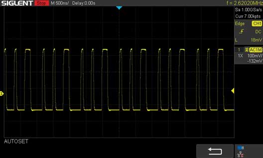
The pulse waveforms demonstrate the time multiplexing of three switch-mode power supplies sharing a single inductor (also known as SIMO power supply).
Deviations from the ideal series of pulse waves can be used to effectively diagnose and fix many problems.
Use Table 6 to diagnose and fix associated problems:
| Input Waveform | Potential Cause | Action | Notes |
| Amplitude is not correct | Inductor open; IN pin open | Disconnect the battery and check all connections with DMM | Repair PCB if needed |
| Duty cycle is not correct (missing pulses) | |||
| SBB0 pulse missing | EN0 shorted to GND | Check SBB0 output for 0 V; disconnect battery and test for conductivity from EN0 pin to GND | PCB may have short |
| SBB1 pulse missing | EN1 shorted to GND | Check SBB1 output for 0 V; disconnect battery and test for conductivity from EN1 pin to GND | PCB may have short |
| SBB2 pulse missing | EN2 shorted to GND | Check SBB2 output for 0 V; disconnect battery and test for conductivity from EN2 pin to GND | PCB may have short |
| Duty cycle is not correct (pulse widths are not correct) | Output voltage select resistors; defective device | Identify SBBx channel associated with incorrect PW and follow associated steps below | |
| SBB0 PW incorrect | RSET_SBB0
shorted to GND (SBB0 VO = 0.5 V) |
Disconnect the battery and test for 40.2 kΩ to GND | Bad/wrong resistor; PCB may have short |
| RSET_SBB0 pin open (SBB0 VO = 5.2 V) | Disconnect the battery and test for conductivity from resistor to RSET_SBB0 pin | PCB may have an open; bad solder connection | |
| Wrong RSET_SBB0 resistor value | Disconnect the battery and test for 40.2 kΩ to GND | Bad/wrong resistor installed | |
| SBB1 PW incorrect | RSET_SBB1
shorted to GND (SBB1 VO = 0.5 V) |
Disconnect the battery and test for 28 kΩ to GND | Bad (shorted) resistor; PCB may have short |
| RSET_SBB1 pin open (SBB1 VO = 5.2 V) | Disconnect the battery and test for conductivity from resistor to RSET_SBB1 pin | PCB may have an open; bad solder connection | |
| Wrong RSET_SBB1 resistor value | Disconnect the battery and test for 28 kΩ to GND | Bad/wrong resistor installed. | |
| SBB2 pulse missing | RSET_SBB2
shorted to GND (SBB2 VO = 0.5 V) |
Disconnect the battery and test for 536 kΩ to GND | Bad (shorted) resistor; PCB may have short |
| RSET_SBB2 pin open (SBB2 VO = 5.5V) | Disconnect the battery and test for conductivity from resistor to RSET_SBB2 pin | PCB may have an open; bad solder connection | |
| Wrong RSET_SBB2 resistor value | Disconnect the battery and test for 536 kΩ to GND | Bad/wrong resistor installed | |
| Waveform distortion rounded rising edge | Bad inductor connection | Reconnect inductor; replace inductor | Bad connection can cause higher line resistance |
Step 3A—Check the output DC voltage: Using a DMM with an internal impedance of 1 MΩ or larger (for example, Fluke 87), measure the voltage at the three outputs of the MAX77642 device. Be sure to connect the negative black lead to the ground and the positive red lead to the associated SBBx channel output OUT pin of the device. If the output pin is not easily accessible, place the leads across the associated output capacitor, COUT.
Use Table 7 to diagnose and fix associated SBB0 and SBB1 (1.8 VDC) output problems:
| Output Voltage Reading | Potential Cause | Action | Notes |
| SBB0/SBB1: zero volts/ no reading | No connection from SBB0/SBB1 to COUT. | Disconnect the battery and test for conductivity from output to COUT | PCB may have an open |
| Output capacitor shorted to ground | Disconnect the battery and check for continuity across the capacitor | PCB may have short | |
| SBB0/SBB1: reading too low (< 1.71 VDC) | Inductor wrong value; inductor saturated; RSET_SBB0/ RSET_SBB1 has wrong value | Disconnect the battery and check for the inductor and/or resistor values | |
| 1.71 V ≥ reading ≤ 1.89 V | No action | Operational | |
| Reading too high (> 1.89 VDC) | RSEL has wrong value | Disconnect the battery and check RSEL value |
Use Table 8 to diagnose and fix associated SBB2 (5.0 VDC) output problems:
| Output Voltage Reading | Potential Cause | Action | Notes |
| SBB2 zero volts/ no reading | No connection from SBB2 to COUT | Disconnect the battery and test for conductivity from output to COUT | PCB may have an open |
| Output capacitor shorted to ground | Disconnect the battery and check for continuity across the capacitor | PCB may have short | |
| SBB2: reading too low (< 4.75 VDC) | Inductor wrong value; inductor saturated; RSET_SBB2 has wrong value | Disconnect the battery and check for the inductor and/or resistor values | |
| 4.75 V ≥ reading ≤ 5.25 V | No action | Operational | |
| SBB2 reading too high (> 5.259 VDC) | RSEL has wrong value | Disconnect the battery and check RSEL value |
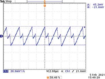
Step 3B—Check the output AC voltage: Using an oscilloscope or DSO, now measure the output ripple (AC) by probing the three outputs of the MAX77642 device. It is recommended to use a differential technique to properly measure the output and avoid RF pickup.
Note: It is recommended that the oscilloscope and probes used have a minimum bandwidth of 200 MHz.
If the circuit is operating correctly, the SBB0 waveform should be a 1.8 VDC (digital) output with a small ripple waveform superimposed on it. Figure 7 shows the ripple waveform.


Use Table 9 to diagnose and fix associated problems for SBB0, SBB1, and SBB2:
| Input Waveform | Potential Cause | Action | Notes |
| Ripple amplitude is too high | Wrong capacitor value; defective capacitor | Disconnect the battery and check all connections with DMM; measure capacitor value | |
| Broadband noise is too high | Load too large; environmental noise | Check load and environmental noise | Use differential probing on output to reduce environmental noise |
| Transition spikes too high | Load inductance too large; input current not adequate | Check line inductance; check input current with scope |
If the circuit is operating correctly, the SBB1 waveform should be a 1.8 VDC (analog) output with a small ripple waveform superimposed on it. Figure 8 shows the ripple waveform.


If the circuit is operating correctly, the SBB2 waveform should be a 5.0 VDC (for LEDs) output with a small ripple waveform superimposed on it. Figure 9 shows the ripple waveform.

Conclusion
This concludes the article series in which prevalidated power supply circuits, both discrete and integrated, for use with the MAX86171-based and MAX86141-based PPG remote patient vital sign monitors were presented. While both the integrated and discrete switch-mode power circuit designs support PPG performance, the integrated solution offers a smaller footprint and reduced part count and is recommended for size-constrained applications.
References
“Designing Accurate, Wearable Optical Heart Rate Monitors.” Analog Devices, Inc., August 2017. Frenzel, Lou. “Improving Remote Patient Monitoring toOvercome Healthcare Limitations.” Electronic Design, November 2020.
关于作者
{{modalTitle}}
{{modalDescription}}
{{dropdownTitle}}
- {{defaultSelectedText}} {{#each projectNames}}
- {{name}} {{/each}} {{#if newProjectText}}
-
 {{newProjectText}}
{{/if}}
{{newProjectText}}
{{/if}}
{{newProjectTitle}}
{{projectNameErrorText}}
最新视频 21


