AN-2578: Using the VREF Pin of RF Amplifier Power Detectors to Monitor Die Temperature
Introduction
On-chip temperature monitoring is a valuable function that ensures safe operation of gallium arsenide (GaAs) and gallium nitride (GaN) radio frequency (RF) power amplifier integrated circuits. Many Analog Devices, Inc., GaAs and GaN power amplifiers come with integrated RF power detectors that are temperature compensated. This application note describes how some of the RF power detector circuitry can be reused to provide an output voltage that is inversely proportional to the on-chip temperature of the device.
Operation Of A Temperature Compensated On-Chip RF Detector
An on-chip RF detector uses a directional coupler placed close to the RF output line. A small portion of the RF power being generated by the amplifier is coupled to this circuit. When the RF output power increases, the signal level on the directional coupler also increases. The coupled RF signal is rectified by a half wave diode rectifier and is low pass filtered. The resulting output is a DC voltage proportional to the RF output level. This voltage has a temperature coefficient that causes it to decrease with increasing temperature. A second circuit is used to compensate for temperature changes in the detector circuit. This VREF circuit is located in a different part of the die and is not coupled to the RF output line. The VREF voltage has a similar temperature coefficient but it is not affected by the RF power level. Subtracting the two voltages yields a temperature stable output voltage that is proportional to the RF power level. In Figure 1, the two 10 kΩ resistors positively bias the two on-chip diode circuits and the op amp circuit is used to subtract VDET from VREF.
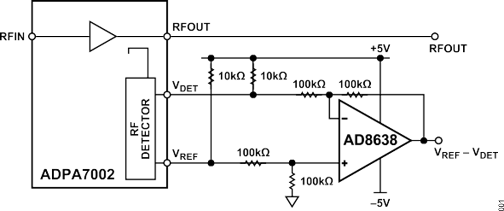
Figure 1. An RF Amplifier with Integrated RF Power Detector.
Figure 2 shows plots of VREF, VDET, and VREF − VDET vs. RF output power for the ADPA7002, an 18 GHz to 44 GHz, 0.5 W power amplifier. The three VDET plots respond to the changing output power and they show a strong temperature coefficient, changing by approximately 150 mV across temperature. The three VREF plots have a similar temperature coefficient but show almost no response to changes in RF output power. The three VREF − VDET plots show a more temperature stable response.
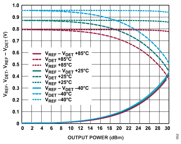
Figure 2. VDET, VREF, and VREF − VDET vs. RF Output Power.
Using VREF As A Temperature Sensor
Because the VREF voltage is being used to compensate for changes in temperature, it then follows that this DC voltage can be used to approximate the temperature on the die. Instead of looking at both VDET and VREF through a typical subtractor circuit, focusing on VREF yields a relationship between output voltage and on-chip temperature.
In Figure 3, the VREF output voltage of the ADPA7002 is plotted vs. base plate temperature with the ADPA7002 evaluation board (ADPA7002-EVALZ) clamped to a hot/cold plate whose temperature is adjusted from −40°C to +85°C. There is a thermal gradient from the hot/cold plate through the evaluation board and the package to the die. Figure 3 shows the following three operating cases:
- Amplifier biased with no RF power present
- Amplifier biased with RF present (POUT = 26 dBm)
- Amplifier biased off (pinch off voltage on gate)
The VREF and VDET circuits are still active and operational in the pinch off case where the gate voltage has been set to a negative voltage low enough to reduce the drain current to zero.
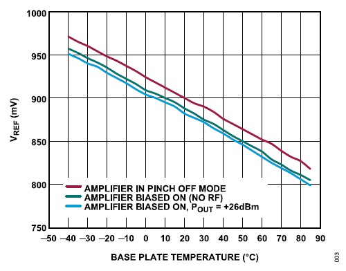
Figure 3. VREF Output Voltage vs. Base Plate Temperature for Three Different Operating Cases.
For each case, a 10°C change in the temperature of the hot plate results in the VREF voltage changing by approximately 12.1 mV or 0.00121 V/°C. Although this temperature coefficient is relatively small and has a large voltage offset, it is consistent over the −40°C to +85°C temperature range, resulting in a range of around 150 mV.
Because the temperature of the hot plate is being forced, the resulting die temperature changes when the power consumption changes. The pinch off case is particularly interesting. With the device biased (VDD = 5 V) and the gate voltage set to a voltage negative enough to pinch off the amplifier, the power consumption becomes very close to zero. For that case, assume that there is little or no thermal gradient from the die to the cold plate. When the temperature on the cold plate is 25°C, the temperature on the die is also approximately 25°C. By putting the device in pinch off mode, the temperature sensor can be calibrated by measuring VREF when the die is at a known temperature such as room temperature (designate it as VREF_PINCHOFF_25°C, 0.894 V in this case).
The general equation that relates output voltage to die temperature follows the familiar y = mx + b format:
VREF = Slope × Temperature + Intercept
where:
Intercept is the output voltage when the temperature is equal to 0°C.
Slope is 1.21 mV/°C.
Although the intercept value can change from device to device, the slope is fairly consistent from device to device. This characteristic enables calibration of the temperature sensor without measuring its slope.
Assuming that the values of the room temperature and the output voltage of VREF when the amplifier is in pinch off mode are known, the values can be added to the equation to calculate the intercept, that is,
Intercept = VREF_PINCHOFF_25°C – (Slope × 25°C)
Intercept = 0.894 – (−0.00121 × 25)
= 0.924 V
Then rewrite the equation for the die temperature (TDIE).
TDIE = (VREF − Intercept)/Slope
= (VREF − 0.924)/−0.00121
Although the pinch off condition is used to calculate Equation 3, which relates output voltage to temperature, this equation applies to all conditions. For example, Figure 2 indicates that when the amplifier is on with an output power of +26 dBm, with the base plate temperature at 25°C, the VREF output voltage is 0.877 V. Adding the output voltage value to Equation 4, the die temperature is higher as expected.
TDIE = (0.9 – 0.924)/−0.00121
= 38.8°C
Conclusions
The VREF output pin, which serves to compensate for the temperature drift in the RF power detection circuit, can be used as an effective die temperature sensor even though the signal has a relatively small temperature coefficient and a large offset voltage. With a slope of 1.21 mV/°C, this voltage can be directly digitized by a 12-bit, 2.5 V ADC (least significant bit (LSB) = 610 μV) to yield a resolution of 0.5°C/bit. If the amplifier can be placed in pinch off mode and brought to a known external temperature, the temperature sensor can be calibrated, thereby providing an indication of the absolute temperature on the die.
作者
