AN-1603: 交流耦合视频驱动程序的直流恢复电路
简介
后视摄像头提供汽车后面区域的通畅视野。这些摄像头通常用于汽车应用,使驾驶员能够安全倒车。安装后视摄像头时,视频源信号和视频驱动电路是典型的交流耦合信号,以对器件提供隔直处理。视频信号的直流电平代表黑色的显示等级,该电平必须恒定才能适应视频处理电路。
本应用笔记说明恢复复合视频信号的正确直流电平的方法。

复合视频信号说明
复合视频信号也称为颜色、视频、消隐和同步(CVBS),是电子中最复杂的波形之一。亮度信息、颜色信息和同步信号组合形成复合视频信号。图2显示全白美国国家电视系统委员会(NTSC)复合视频信号的典型波形。

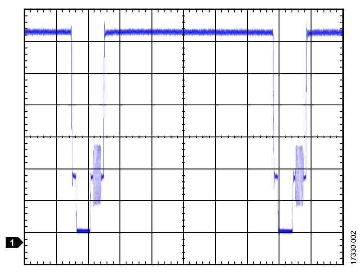
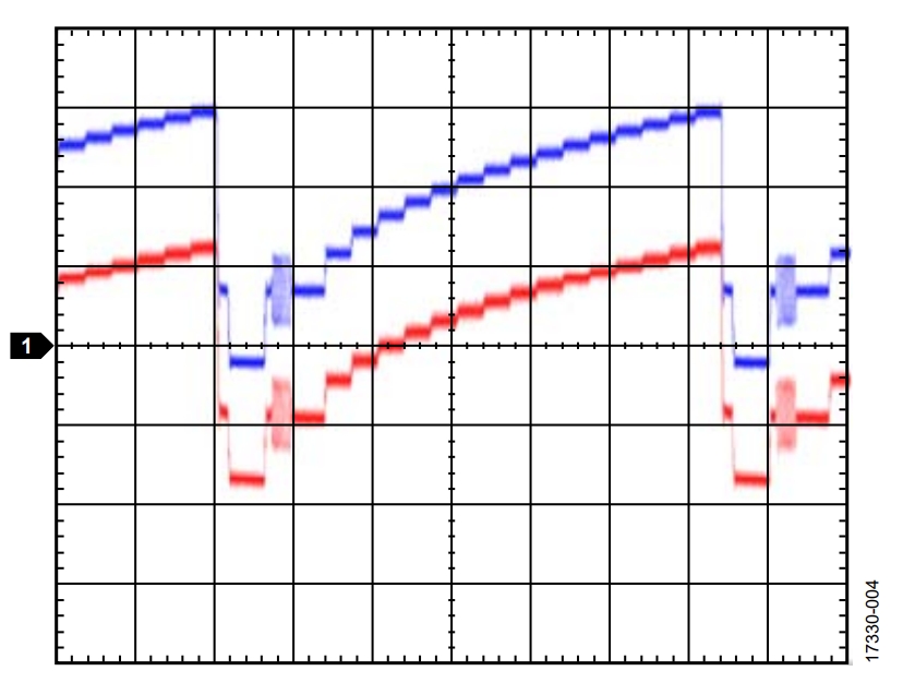
在图2中,视频信号相当于一条水平扫描线。一条扫描线由一个有效视频部分和一个水平消隐部分组成。有效视频部分包含图片的亮度信息(亮度)和颜色信息(色度)。亮度是信号的瞬时振幅,色度是正弦波。为了识别图片的颜色(黄色、青色、绿色、品红、红色和蓝色),可比较正弦波相位和颜色同步相位间的差异。色度被施加到亮度信号上。此复合信号如图3所示,图中显示了电视彩条的扫描线。


有效视频部分的幅度对应于色彩量(饱和度),色度和色同步之间的相位差表示颜色的色调。水平消隐部分包含水平同步脉冲以及位于同步脉冲上升沿后面的色同步(称为后沿)。
交流耦合
视频源通过输出电容(CS)进行交流耦合。此方法可防止设备受到潜在损坏,如电池意外短路或直流电流而导致的电源连接。
CS存储电压信号的平均值。视频内容会影响视频波形的平 均电压信号,例如,黑色电平随场景亮度而变化。根据视 频内容,如NTSC或逐行倒相制(PAL),必须考虑一个时间 常数,因为 CS 和放大器的高输入阻抗相结合产生的滤波器 的时间常数为 τ = R × CS,截止频率 (fC) 计算如下:

CS和R值是可能导致信号幅度下降的变量。
下降是从视频的左侧沿到右侧沿的亮度变化,这会导致显示器上可见暂时闪烁或淡入淡出。下降幅度必须低于人类感知。要最大限度地减少下降,交流耦合电路的时间常数必须尽可能短。为了补偿短时间常数,可在电路中添加一个或多个电容。因此,必须适当调整电容的值。在选择正确的电容时,低泄漏比等效串联电阻(ESR)的指标更重要。
要正确设置输入共模电平,滤波器或驱动器输入需要一个 钳位和偏置电路。
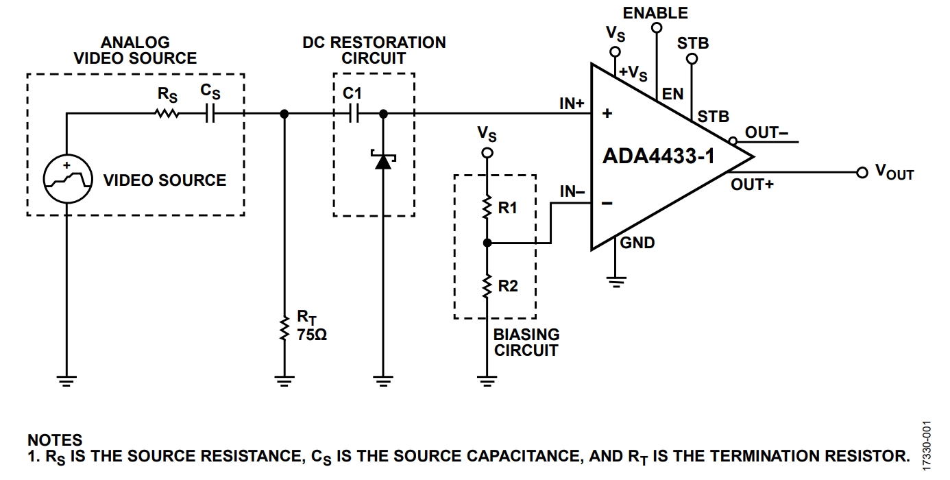
采用肖特基二极管的直流恢复
对视频设备的输出进行交流耦合时,直流内容会丢失。要恢复直流偏置电平,视频源的交流耦合输出必须使用直流恢复或箝位电路箝位至基准直流电压。使用交流耦合时,最大限度地减小电源需求的一种方法是使用肖特基二极管进行直流箝位,如图1所示。在此应用中使用肖特基二极管比普通硅或锗二极管具有显著的优点。肖特基二极管具有低正向电压和快速恢复或开关时间。射频(RF)肖特基二极管的导通电压低。具有30 mV导通电压的二极管在单电源应用中可提供令人满意的结果。
当耦合电容上的负载较高时,如ADA4432-1输入阻抗缓冲器,耦合电容上的平均电压沿正向电压向上渗透。低电压肖特基二极管提供同步端箝位功能,如图4所示。当二极管的阴极电压高于零时,二极管用作单向开关。因此,信号的最低部分被强制为基准电压,即肖特基二极管阳极的电压电平。耦合电容的值也取决于终端电阻。如果75 Ω终端电阻与肖特基二极管并联,则耦合电容必须很大(~100 μF或更大)。如果终端电阻高,则为1 μF或更低的耦合电容是合适的。此电路有一个缺点,即由于二极管导通电流,同步端有轻微的损失。因此,在系统中低漏电流比高ESR更重要。
ADA4432-1的运行电压为3.3 V,放大器输出的增益为2。因此,典型的1 V p-p NTSC复合信号具有以下设计余量:

其中:
VOH 是高电压输出。
VOL是低电压输出。

结论
将视频源交流耦合至接收器时,恢复复合信号的适当直流电平对于提供已传输视频信号的正确亮度至关重要。因此,务必考虑正确的电容值以避免电压幅度下降,并使用低电压肖特基二极管以减少同步端损失。直流箝位还可防止改变场景时同步信号漂移,因为二极管为同步端提供恒定基准电压。
作者
