ADGS6414D
推荐用于新设计0.56Ω On Resistance High Density Octal SPST Switch
- 产品模型
- 2
产品详情
- 0.56Ω typical on resistance
- High continuous current of up to 768 mA
- Flat RON across signal range of 0.004 Ω
- THD of −127 dB at 1 kHz
- Route through pins for digital signals and supplies
- Integrated passive components
- SPI with error detection
- Guaranteed break-before-make switching, allowing external wiring of switches to deliver multiplexer configurations
- Fully specified at ±20V and +36V
- 1.8 V logic compatibility with 2.7 V ≤ VL ≤ 3.3 V (excludes SPI read back to a 1.8V device)
- 4 mm × 5 mm, 30-terminal LGA
The ADGS6414D contains eight independent, low on-resistance, single-pole/single-throw (SPST) switches in a 4mm × 5mm, 30-terminal LGA package.
The ADGS6414D enables higher channel density in systems where printed circuit board space is constrained or existing system form factors restrict expansion.
When using SPI daisy-chain mode, the unique route through pins provide considerable space savings when multiple ADGS6414D instances are combined to design very high channel count systems, such as large switching matrices and fanout applications. The integrated supply decoupling capacitors and SDO pullup resistor further increase the space savings and reduce printed circuit board complexity.
The low on-resistance (0.56Ω typical) of each switch channel allows for higher current density in systems where heat dissipation is an issue, and the on-resistance profile of the switch channels is exceptionally flat over the full-analog input range, which ensures good linearity and low distortion when switching precision analog signals.
Each switch has an input signal range from VSS to VDD – 2V. When on, each switch conducts equally well in both directions, and in the off condition, signal levels up to the supplies are blocked.
The SPI has robust error detection features, such as cyclic redundancy check (CRC) error detection, invalid read and write address detection, and SCLK count error detection.
PRODUCT HIGHLIGHTS
- The SPI removes the need for parallel conversion, logic traces, and reduces the general-purpose input/output (GPIO) channel count.
- Daisy-chain mode removes additional logic traces when multiple devices are used.
- Route through of digital signals and supplies eases routing and allows for an increase in channel density.
- Integrated passive components eliminate the need for external passive components.
- CRC error detection, invalid read and write address detection, and SCLK count error detection ensure a robust digital interface.
- CRC, invalid read and write address, and SCLK error detection capabilities allow for the use of the ADGS6414D in safety-critical systems.
- Pin for pin replacement for the ADGS1414D and ADGS2414D.
APPLICATIONS
- Automatic test equipment
- Solid-state relay replacement
- Relay replacement
- Instrumentation
- Data acquisition
- Avionics
- Audio and video switching
- Communication systems
参考资料
数据手册 1
用户手册 1
视频 1

ADI 始终高度重视提供符合最高质量和可靠性水平的产品。我们通过将质量和可靠性检查纳入产品和工艺设计的各个范围以及制造过程来实现这一目标。出货产品的“零缺陷”始终是我们的目标。查看我们的质量和可靠性计划和认证以了解更多信息。
| 产品型号 | 引脚/封装图-中文版 | 文档 | CAD 符号,脚注和 3D模型 |
|---|---|---|---|
| ADGS6414DBCCZ | 30-lead LGA (4 mm x 5 mm x 1.63mm) | ||
| ADGS6414DBCCZ-RL7 | 30-lead LGA (4 mm x 5 mm x 1.63mm) |
这是最新版本的数据手册
软件资源
找不到您所需的软件或驱动?
申请驱动/软件硬件生态系统
评估套件
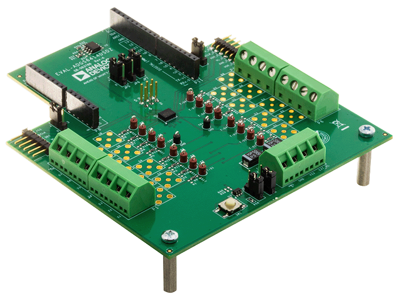
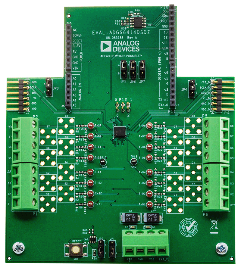
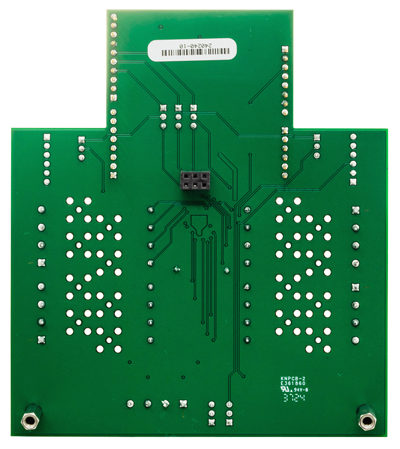
评估 ADGS6414D 0.56 Ω 导通电阻高密度八路 SPST 开关
资料
最新评论
需要发起讨论吗? 没有关于 ADGS6414D的相关讨论?是否需要发起讨论?
在EngineerZone®上发起讨论